Spintronics harnesses the exotic electrons of topological insulators
Researchers from Unité Mixte de Physique CNRS Thales and CEA INAC SP2M, in partnership with the CASSIOPÉE beamline, demonstrate the potential of recently discovered topological insulator α-Sn for room temperature spintronics. They observe a large spin to charge current conversion (SCC) in experiments of resonant spin pumping into the Dirac cone (DC) with helical spin polarization of the elemental topological insulator (TI) α-Sn. The DC associated to the surface states was evidenced during the growth by ARPES on the CASSIOPÉE beamline. The results have been published in Physical Review Letters.
Most spintronics devices are today based on the manipulation of spin currents that do not carry electrical charges but can be described as equal flows of electrons with opposite spins in opposite directions. Basic spintronics operations are the creation of spin currents from charge currents (electrical currents) and the detection of spin currents by transforming them into charge currents, in other words, conversions between charge and spin currents. Classical spintronics generally uses magnetic materials for these conversions, but it now appears that they can also be obtained by harnessing the spin-orbit coupling (SOC), the relativistic correction to the equation of quantum physics, that can be significantly strong in materials containing heavy atoms. A typical example of SOC effect is the spin Hall effect (SHE) of heavy metals by which a charge current can be converted into a transverse spin current and the inverse spin Hall effect (ISHE) for the inverse conversion. Today, it turns out that a more efficient conversion can be obtained by exploiting the SOC-induced properties of a two-dimensional electronic systems at some surfaces and interfaces, the so-called Rashba interfaces and the surfaces or interfaces of new materials called topological insulators (TIs). In this case the charge to spin current conversion is called Edelstein Effect (EE), who first described it, and inverse Edelstein effect (IEE) for the reverse effect.
Here we present spin pumping experiments on thin α-Sn (0 0 1) films, a recently characterized new type of TI. They reveal an unprecedented SCC efficiency by IEE. The SCC by EE and IEE is promising for the generation and detection of spin currents in spintronic devices. InSb(001)/α-Sn(001) and InSb(001)/α-Sn(001)/Ag/Fe samples with 30 monolayers (ML) thick α-Sn(001) layers were grown by molecular beam epitaxy inside the CASSIOPEE beamline of the synchrotron SOLEIL. The growth inside the beamline UHV system allows us to check by ARPES (Fig. 1a) if the DC subsists after covering α-Sn by thin Ag layers and before growing the complete structure (Fig1b) and taking it off for spin pumping. In the ARPES images of Fig. 1a, a DC is clearly seen at the free surface (top surface) of α-Sn(001), and subsists when α-Sn is covered with even 1.2 nm of Ag.
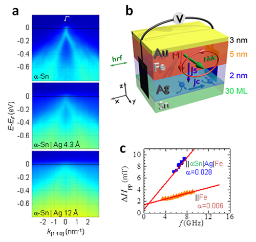
(a) ARPES characterization of the interfaces states of α-Sn (0 0 1) films covered by Ag. Top: ARPES intensity plots of the DC along [110] on the free surface of α-Sn (approximately 30 ML thick). Below: ARPES plots after covering a-Sn by 4.3 or 12 Å of Ag. The intensity is color coded with the same color scale in each panel (arbitrary units).The DC subsists if α-Sn is covered by Ag, and it can still be seen when the Sn/Ag interface is buried below 12 Å of Ag. (b) Schematic for spin pumping into α-Sn by ferromagnetic resonance (FMR) of a Fe layer. (c) Broadband frequency dependence of the peak-to-peak FMR linewidth when the magnetic field H is applied along the [1 0 0] direction of the InSb substrate for InSb/Fe/Au (reference for the Fe layer) and InSb/αSn/Ag/Fe/Au samples. The effective damping coefficient of Fe, proportional to the slopes, is definitely larger with the α-Sn/Ag interface (α=0.028 compared to 0.006 for the reference, which shows the strong spin absorption by the α-Sn/Ag interface).
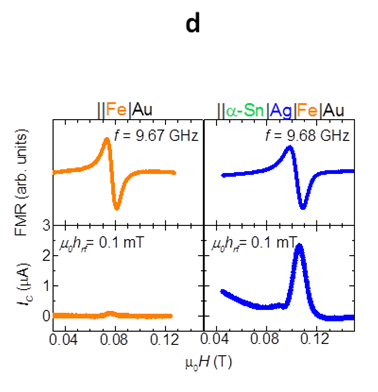
The correlation between the existence of a DC at the surface of α-Sn covered by Ag and a large Spin to Charge Conversion is confirmed by the spin pumping experiments (Figs. 1(c) and 1(d)).
This result draws a promising avenue for room temperature spintronic devices even though the theoretical picture of a-Sn TI properties is not completely clear yet, opening the road to further experiments and better understanding of this new TI.