Self-assembled vertically aligned epitaxial ferromagnetic alloy nanowires: a combinatorial approach
Researchers at the Paris NanoSciences Institute (CNRS-UPMC), in collaboration with groups at SOLEIL and UVSQ, have developed a new technique for growing epitaxial alloy nanowire arrays in a matrix. These results are published in the journal ACS Nano.
Heteroepitaxy1 of horizontal structures is a well-established way of obtaining coherent stacking of different materials and thus developing systems with new properties of interest in many areas of physics, including optoelectronics, magnetism and spin electronics. In recent years new types of vertical epitaxial heterostructures have emerged, where a material grows in the form of nano-pillars or nanowires epitaxially in the matrix of another material. This geometry might lead, for example to progress in the field of multi-functional nano-composites, or even to control deformations along the wire axis, etc.
A new technique for obtaining alloy nanowires
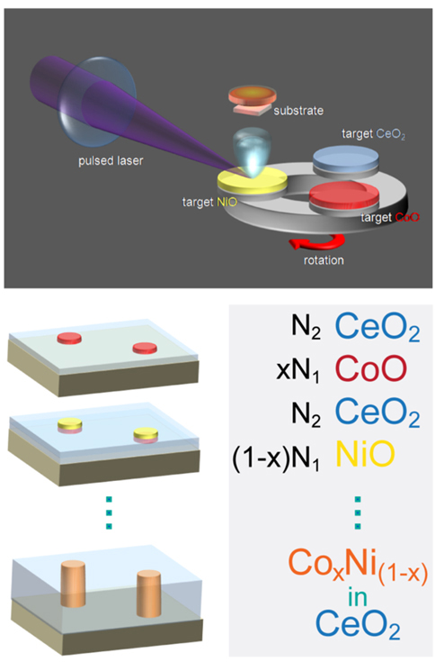
The production technique used in this study is based on a combinatorial approach to pulsed laser ablation, illustrated in Figure 1. By sequentially depositing in sub-monolayers, controlled amounts of Co, Ni and cerium oxide, on a SrTiO3(001) substrate, it is possible to obtain self-assembled nanowire arrays 4 nm in diameter of CoxNi1-x alloy in a monocrystalline CeO2/SrTiO3(001) matrix.
Several techniques to characterize nanowires
The metallic character of these wires has been shown by X-ray absorption measurements on the Ni and Co K-edge, carried out on the SAMBA beamline. Chemical mapping of the samples, by filtered transmission electron microscopy on the Ni and Co L-edges, has shown nanowire growth within the matrix and confirmed the formation of an alloy: Co and Ni are clearly present simultaneously in the nanowire. These results are backed-up by the absorption X measurements at the K-edge: the structure around the atoms of nickel and cobalt has been modified at the same time and depending on the ratio between the two species.
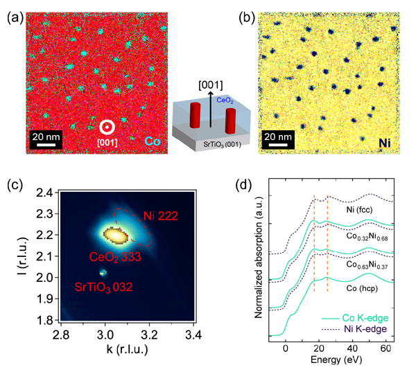
The resulting system is epitaxial: CoxNi1-x is in cube-on-cube epitaxy with the matrix, which is itself epitaxially grown on the substrate. This could be established by high resolution transmission electron microscopy and X-ray diffraction measurements, notably on the SIXS beamline.
Programmed creation of nanowires
The ability to control the composition by the sequence used for growth has been checked: the Co/Ni ratio in the wire is indeed as programmed. This allows the magnetic anisotropy of the nanowire obtained to be adjusted: by starting with pure nickel and increasing the proportion of cobalt, thus obtaining nanowires with ever greater magnetic anisotropy.
Theoretically, this method can be applied to other compounds and thus control a physical property that depends on the composition of the epitaxial nanowires or nanopillars. In the case of cobalt-nickel alloys, very soon it will be possible to optimize the Co/Ni ratio while maintaining a cubic crystal structure. This is not possible on the large scale for very high percentages of Co: the system then transits to the hcp phase. The situation may be different for very small diameter nanowire arrays grown on substrates.
In general, there is still much to learn about epitaxy, its limitations and adaptation to this type of nano-object.
These studies were funded by C’nano IdF and ANR (ANR-2011-BS04-007-01).
1 – Epitaxy refers to the deposition of an overlayer on a crystalline substrate, where the overlayer is in registry with the substrate. (Some researchers also think there must be one or more preferred orientations of the overlayer with respect to the substrate for this to be termed epitaxial growth).This can be divided into homoepitaxy, where a crystalline film is grown on a substrate or film of the same material and heteroepitaxy in which a crystalline film grows on a crystalline substrate or film of a different material (based on Wikipedia).