Hydrogen-induced nanotunnel opening below the surface of a semiconductor, Silicon Carbide
Nanostructuring a surface is a key and mandatory engineering step toward advances in nanotechnology. A team of french and italian scientists and of a franco-american company has just shown that hydrogen/deuterium (H/D) induces the opening of nanotunnels below the surface of an advanced semiconductor, silicon carbide (SiC). Such a finding is an especially interesting one, particularly in views of the specific properties of SiC. These investigations have been performed using advanced experimental tools such as synchrotron radiation and vibrational spectroscopy techniques, and state-of-the-art theoretical simulations. Depending on the H/D SiC surface exposures, these nanotunnels undergo through a sequence of semiconducting/metallic/semiconducting transitions. Such nanotunnels open very promising prospects toward applications in electronic, chemistry, storage, sensors and biotechnology.
One of the key steps in nanotechnology is our ability to engineer and fabricate low-dimensional nano-objects, such as quantum dots, nanowires, two-dimensional atomic layers or three-dimensional nano-porous systems. Silicon carbide (SiC), a wide band-gap semiconductor, offers fascinating structural, thermomechanical, electronic, and chemical properties with a vast range of advanced applications including high-power, high-frequency, and high-temperature electronics devices and sensors. SiC has also a remarkable biocompatibility making it useful for biomedical applications. It is a substrate especially suitable for the growth of epitaxial graphene with subsequent very promising potential applications in electronics and spintronics. Strain/stress interplay is the dominant driving force in SiC surface ordering, leading to more than 10 different surface reconstructions ranging from Si-rich to C-rich cubic SiC surfaces, and to the self-formation of highly stable massively parallel passive or active atomic lines and nanowires at the surface. Most interestingly, the interaction of H/D atoms with the Si-rich 3C-SiC(001)-3x2 surface reconstruction leads to surface metallization, which is the first example of H/D-induced metallization of a semiconductor surface [1]. Although there are some examples of voids or nano-cavities generated at a surface or below, most are in the µm or sub-µm scales, and none exhibit spatial ordering.
Here we report the 1st evidence of nanotunnel opening taking place within the subsurface region of a semiconductor, SiC, as depicted in Figure 1. Such an effect is induced by selective hydrogen/deuterium interaction at the surface, which possesses intrinsic compressive stress. This finding is established combining ab-initio and vibrational computations using the VASP method within the MedeA® environment, and vibrational spectroscopy & synchrotron-radiation-based photoemission experiments.
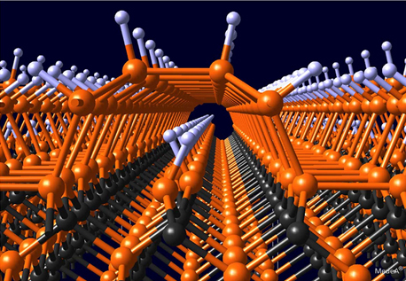
Hydrogen/deuterium-induced puckering of the subsurface Si atoms marks the critical step in this nanotunnel opening. Depending on hydrogen/deuterium coverage, the nanotunnels are either metallic or semiconducting as identified by density of states (DOS) calculations and photoemission experiments performed on the TEMPO beamline. The experimental system is optimized to monitor live the electronic properties during hydrogen exposure, thereby leading to identify the semiconducting/metal/semiconducting transition as a function of hydrogen exposures as shown in Figure 2 comparing calculated and measured DOS, which appear to be in excellent agreement.
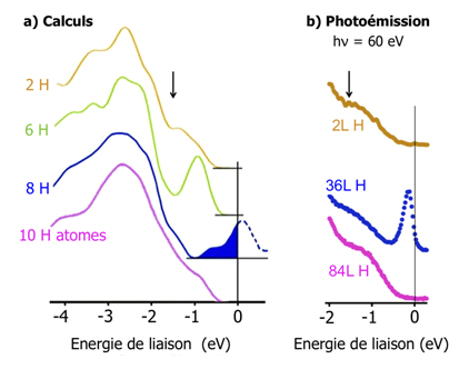
The vibrational frequencies for the clean and hydrogen-covered 3C-SiC(001)-3x2 surface measured by high-resolution electron energy loss spectroscopy (HREELS) are also in excellent agreement the computed ones. Dangling bonds generated inside the nanotunnel offer a promising template to capture atoms or molecules. These features open nano-tailoring capabilities towards advanced applications in electronics, chemistry, storage, sensors or biotechnology. Understanding and controlling such a mechanism open routes towards selective surface/interface functionalization.
Reference :
1- V. Derycke, P. Soukiassian, F. Amy, Y.J. Chabal, M. D’angelo, H. Enriquez, M. Silly
Nanochemistry at the atomic scale revealed in H-induced semiconductor surface metallization
Nature Materials 2, 253 (2003)