Optimization of 2D material-based devices. How to visualize electric fields in situ to boost the performance of tomorrow's LEDs
2D materials are excellent candidates for light emission in LED-type components. Furthermore, combining several of these materials with different properties (metal, insulator, semiconductor) theoretically makes it possible to obtain complex components that combine these properties. To function, these components must be connected to electrodes. But where exactly should the electrical voltage be applied?
To answer this question, a team from the Paris Institute of NanoSciences used the ANTARES beamline to probe operando the distribution of the electric field within a heterostructure composed of two semiconductors.
Two-dimensional (2D) materials, such as transition metal dichalcogenides (TMDs) (e.g., MoS₂, WSe₂, and their derivatives), exhibit strongly enhanced excitonic effects due to the robust Coulomb coupling between electron-hole pairs. This makes them outstanding candidates for light emission in devices such as LEDs. A second key advantage of this materials platform is the ability to assemble these materials without epitaxial constraints. In theory, this allows for the combination of materials with diverse properties—metals, insulators, and semiconductors with tunable bandgaps—to fabricate complex devices. The entire structure is ultimately connected to electrodes, which serve to inject charges or modulate the potential profile. However, a critical challenge remains: the voltage must be applied in the right location! In these structures, the energy landscape is influenced by edge effects, doping, flake thickness, defects, and above all interfaces. In this study, a team from INSP uses the ANTARES beamline to operando probe the electric field distribution within a heterostructure composed of two semiconductors.
In optoelectronic devices, electrodes are used to inject the current/energy necessary for device operation. In the context of LEDs, applying a bias is essential to inject holes into the valence band while electrons are resonantly injected into the conduction band. When these energy conservation rules are fulfilled, charges can be injected into the optically active semiconductor, enabling light emission. However, the turn-on voltage for an LED can be significantly larger than the material’s bandgap if an electric field is also applied to the intermediate material between the electrode and the optically active layer. This results in power efficiency losses, which must be mitigated. Therefore, the localization of the electric field is critical, and tools to measure the field distribution operando are essential.
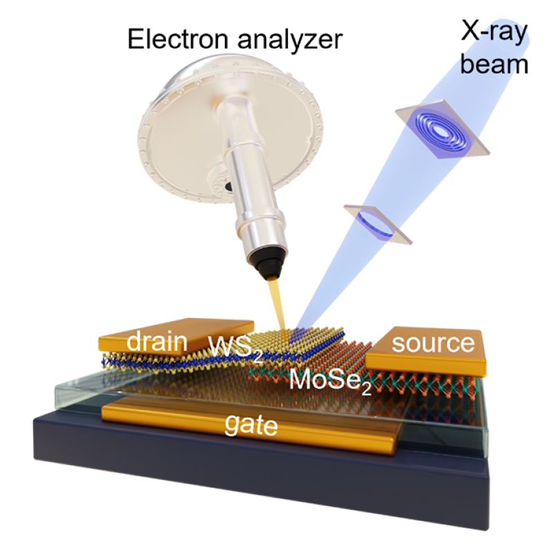
In this study, researchers used the nanobeam from the ANTARES beamline, which acts as a local probe of the electrostatic landscape. In practice, the synchrotron beam is first focused using a Fresnel lens, as depicted in figure 1, generating a 700 nm spot at the sample level. The sample is then scanned perpendicularly to create an image. For each spot, a photoemission spectrum is acquired, allowing researchers to track how a given core level shifts upon bias application. What makes this method particularly relevant for van der Waals heterostructures is its atom selectivity, enabling the potential experienced by different materials to be tracked as long as their compositions differ by at least one atom.
Here, the method has been applied to a semiconductor heterostructure composed of WS₂ and MoSe₂. Since these materials differ in carrier mobility and density, their conductivities can vary significantly. In the overlapping region, two extreme cases can be anticipated:
- A bulk-like scenario, where the potential experiences a gradient that is relatively insensitive to the presence of an interface.
- A scenario where one layer imposes its potential, and the bias drop is fully accumulated on the second material.
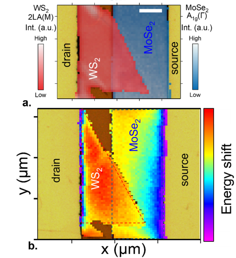
Samples were prepared using scotch-tape exfoliation of the flakes and conventional photolithography for the electrodes, ensuring that device fabrication is not specific to the experimental setup. Raman microscopy can be used to identify the different flakes within the heterostructure, as shown in figure 2a.
Scanning photoemission microscopy (SPEM) measurements reveal that, in the targeted heterostructure, the flake interface does not accumulate the bias drop, while the contacts do (i.e., mapping reveals presence of Schottky barrier) The results also demonstrate that gate effects are possible in such heterostructures (figure 2b) and can tune the potential of both the top and bottom flakes. The shape of the flakes and electrode localization clearly influence the magnitude of the gate-induced energy shift, emphasizing the need for careful device geometry design to maximize efficiency.
The next step will be to expand this type of study to other 2D materials with stronger asymmetry in conductivity, such as metal-semiconductor van der Waals heterostructures. The outcome of these studies will be the identification of design and fabrication rules to maximize the effects of bias application.