ANTARES
As one of the latest instrumentation built at SOLEIL, ANTARES beamline offers a spectroscopic non-destructive nano-probe named k-space nanoscope to study advanced materials using angle resolved photoemission spectroscopy with nano-scale lateral resolution (nanoARPES).
Introduction
This innovative scanning photoemission nanoscopy combines the extreme focalization of the polarized incident light with linear, deflexion and angle sweeps to perform precise electronic band structure with high energy, angular and lateral resolution. The imaging of selected electronic bands with a given binding energy and momentum thorough the investigated samples can be straightforwardly linked with a complete punctual band structure determination in selected areas of the samples, where the electronic heterogeneities are spotted. This exhaustive electronic characterization of the samples can furthermore be in situ combined with a detailed chemical imaging of a wide variety of materials by using high energy resolution photoemission (HRPES) of chemically shifted core level and X-ray absorption (XAS). Complementary, compatible techniques as resonant photoemission (ResPES) and photoelectron diffraction in energy (PhD) and angular (XPD) scanning modes are also fully implemented at the ANTARES beamline. The highly developed automatic software facilitates an effortless operation to carry out studies using a multi-technique approach.
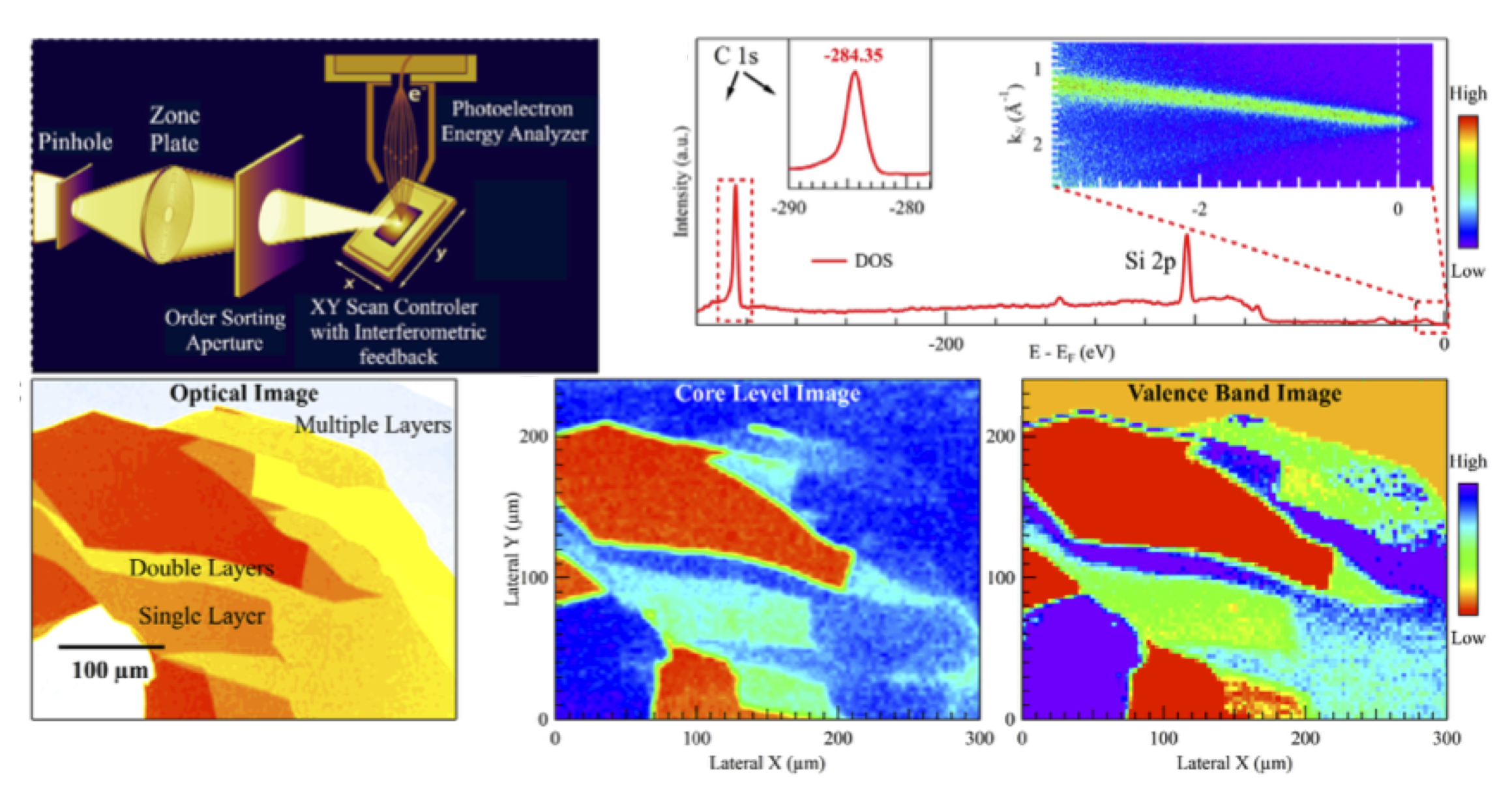
ANTARES setup (top left) and imaging of exfoliated graphene on SiO2 using an (1) optical microscope (bottom left panel); (2) carbon 1s photoemission peak (bottom central panel) and (3) nanoARPES of the Dirac electronic states at the Fermi level (bottom right panel). In optical imaging, the graphene becomes visible only when it is placed on top of a silicon wafer covered by SiO2 films of a given thickness. However, for the chemical and electronic imaging the photoemission intensity of a chosen core level and a given valence band electronic states are respectively measured sequentially throughout the whole sample.
The goal of this website is to present a complete and comprehensive description of the ANTARES beamline (BL) at the “Synchrotron SOLEIL”. In particular, the current performance of the ANTARES installations, the home scientific research as well as the scientific collaborations, associated user community and highlights are briefly described.
History of the ANTARES beamline
The project to build this Angle Resolved Electron Spectroscopy (ARPES) related BL at SOLEIL has its origin on the successful activities accomplished by the former BL at LURE, named “SU8” dedicated to perform classical ARPES, high resolution core levels (CL) and photoemission and Photoelectron Diffractions (PhD) experiments. After the cloture of LURE at the end of 2003, a detailed document describing the new LB was produced in June 2007, whose evaluation and aprovation by the SOLEIL directors, ensured the green light for the construction of the new BL installation, at the brand new SOLEIL Campus. Due to the technical complexity associated to the microscopic aspects of the new BL, its construction was recommended among the Phase II beamline SOLEIL portfolio.
The new BL ANTARES was designed, built and commissioned at SOLEIL from 2007 until December 2009. The acronym ANTARES stands for «Analysis Nano-spoT Angle Resolved photoEmission Spectroscopy». The complete design of this BL was fully accomplished by SOLEIL teams and no external company was contracted to help in the conception, drafts and outlines required for its construction. The firsts expert users were welcomed at the BL during the last two months of 2009. Finally, the BL was declared fully operational and open to the General Users in January 2010. Even if the first years of operation considerable optimization have to be done due to the inherent early development of this new k-space nanoscope, the ANTARES BL has become the "First nanoARPES User Facility" open to the scientific and industrial community.
Beamline news
All beamline news
Electronic structures of quantum materials - Shining new lights on the fractional quantum (...)
SOLEIL Highlights 2024
Team
* External service provider, temporary or collaborator
Employment
Click here to access to the SOLEIL employment web page
Technical data
- Energy range
-
12-1000 eV (without Zone Plates)
95-1000 eV (with Zone Plates)
- Energy Resolution (∆E/E)
-
>20000 (10-150 eV)
>10000 (150-1000 eV)
- Source
-
- HU256 (256 mm period) electromagnetic
- HU60 (60 mm period) permanent magnet – type AppleII
- Variable polarization light: lineal H and V, circular
- Flux at the first optical element
-
1.2•10+15 Photons/s/0.1% BP @ 100 eV
- Optics
-
- PGM without entrance slits, using plane gratings with varied line spacing
(VLS) and variable groove depth (VGP)
2 gratings (600 tr/mm and 1300 tr/mm)
- Double Pseudo-Wolter (Focus on Sample and Using Zone Plates)
- 2 Fresnel Zone Plates
- Sample Environment
-
- 5 axis High precision sample manipulator (better than 1 micron resolution)
- Scan sample Manipulator (x,y,z) (resolution better than 5 nm)
- The sample can be cooled down thanks to a liquid He cryostat.
- Flux on sample
-
-Without Zone Plate:~ 5•10+12 Photons/s/0.1% BP (@ 100 eV) (E/ΔE = 10000)
-Using ZP : 5•10+10 -10+11 Photons/s/0.1% BP
- Detectors
-
- High energy and angle resolution kinetic energy electron analyzer
(MB Scientific, type A-1)
- Low Energy Fluorescence Detector
Scientific opportunities
The spatially resolved ARPES (nanoARPES) is a development of conventional ARPES technique achieved with the focusing of light on the sample into the spot with submicron sizes. This development is used in research of essentially small samples, for example, heterostructures build of flakes of 2D materials, micro-crystals or polycrystalline samples, different crystal termination, domains in electronic structure.
ANTARES is delivering the nanoARPES technique to user community since 2010, up to now the instrument was used with samples of various types, and that was useful to accumulate the specific experience
Available techniques
- Scanning electron photoemission microcopy (SPEM) for core levels
- Nano-ARPES
- Angle Resolved Photoemission Spectroscopy at submicrometer scale
- Fermi Surface Mapping
Industry