Quantum multilayer materials – WSe2/BiFeO3 heterostructures for future non-volatile memories?
The purpose of this work is to study the dependence of the electronic structure of WSe2 – which determines all its properties – with the direction of the electric polarization of a ferroelectric compound on top of which it is deposited.
The WSe2 compound belongs to the transition-metal dichalcogenides family (MX2, M = Mo, W, Pt, … and X = S, Se, Te). These materials exhibit a mainly bidimensional structure with MX2 planes in which each transition-metal atom is covalently bonded to two chalcogen atoms. The tridimensional structure of these materials consists of the stacking of these elementary planes which are weakly bonded together thanks to van der Waals interactions. Due to their electronic structure, these materials have a strong potentiality for applications in the fields of electronics, photonics and spintronics. Moreover, because of their bidimensional nature, the electronic properties of these materials can be easily modified by the vicinity of another material or with an external stimulation.
In this study, resulting from a collaboration between the CASSIOPEE beamline team, the C2N (Palaiseau), the CNRS-Thalès UMPhy lab (Palaiseau) and IRIG-SPINTEC (Grenoble), WSe2 has been deposited on a BiFeO3 substrate. This material is ferroelectric, i.e. it exhibits a spontaneous macroscopic electric polarization due to the spatial shift of some atoms in the structure. Then, the influence of the direction of this BiFeO3 electric polarization on the WSe2 electronic structure has been studied.
Heterostructure fabrication
Up to now, this kind of study has been performed only on some small transition-metal dichalcogenides flakes obtained by exfoliation and poorly characterized. Here, some very good quality WSe2 films, obtained by epitaxy, have been used.
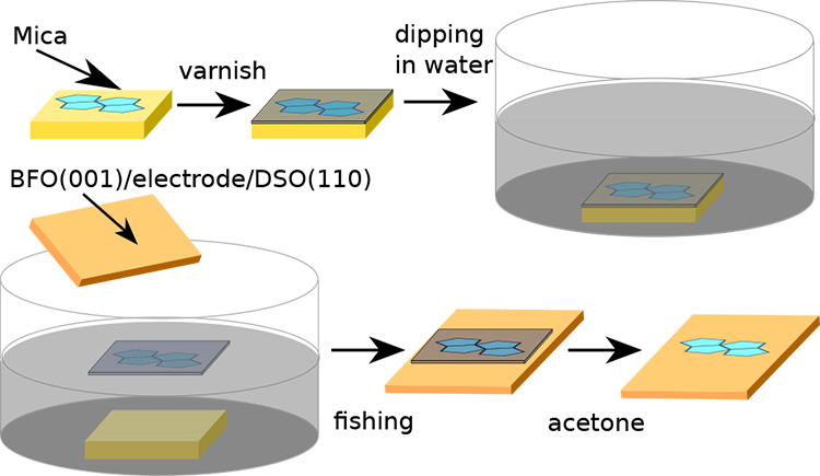
Thin films of SrRuO3 (SRO) or La0.7Sr0.3MnO3 (LSMO) have been deposited on DyScO3 substrates and covered with BiFeO3 (BFO) films. The electric polarization of BFO is then perpendicular to the surface and, depending on the intermediate layer nature (SRO or LSMO), it points either towards the inside (down) or towards the outside (up) of the stacking. At the same time, some 2 or 3 atomic layers thick WSe2 films are epitaxially grown on mica substrates and subsequently wet-transferred on BFO layers. Stackings in which WSe2 experiences a down or up electric polarization are then obtained.
Photoemission measurements
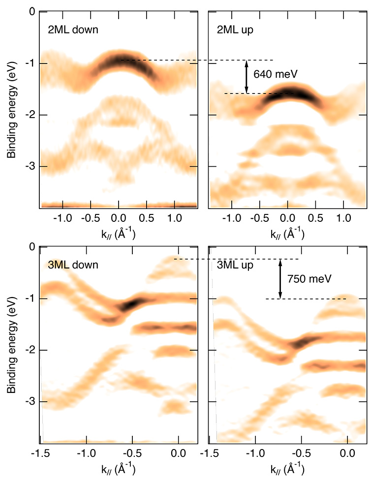
The electronic structure of SRO/BFO/WSe2 and LSMO/BFO/WSe2 stacks has been studied by photoemission on the CASSIOPEE beamline for 2 and 3 atomic layers thick WSe2 films. The photoemission technique, based on the photoelectric effect, allows to experimentally measure the band structure which determines in solids the allowed energies (E) for valence electrons as a function of their propagation direction (given by the wave vector k).
The results obtained on the two types of stackings (Fig. 2) show that the band structure is shifted by 640 and 750 meV between the two electric polarization directions for, respectively, 2 and 3 atomic layers thick WSe2 films.
Then, as a function of the BFO electric polarization direction, the WSe2 electronic structures are very different and could be easily differentiated thanks to electric conductivity measurements of the stackings.
Perspectives of applications : non-volatile information storage devices
This kind of heterostructure behaves as a ferroelectric field-effect transistor and could be used to make non-volatile information storage devices with a strong ON/OFF contrast.
The information writing would be achieved by applying a voltage which can switch the ferroelectric polarization while the reading would be done thanks to an electric transport measurement which is sensitive to the electronic structure differences.
This study forms a large part of Raphaël Salazar's thesis.
* Epitaxy: technique used to grow few nanometers thick single-crystalline films. For that purpose, atoms are deposited on a perfectly polished single-crystalline surface – the substrate – which behaves as a kind of mold for the ordered growth of the thin films.