Transition metal dichalcogenides - Evolution of their electronic structure from two- to three-dimensional
Ever since the discovery of graphene, research on two-dimensional (2D) materials is ongoing a tremendous effort. Along with this trend, transition metal dichalcogenides (TMD) are extremely promising for possible technological applications at the monolayer limit, in the field of optoelectronics or for the development of ultimately small transistors. The three-dimensional (3D)-solid is obtained by stacking these monolayers.
But how does the electronic structure transform from two-dimensional material, in a monolayer, to three-dimensional in the crystal bulk?
That's the question scientists from C2N (University Paris-Saclay, Palaiseau), SPINTEC (University Grenoble-Alpes, CEA et CNRS, Grenoble), the New Technologies Research Centre (University of West Bohemia, Pilsen, Czech Republic) and the IPR (Rennes) set out to answer, in collaboration with the team of CASSIOPEE beamline, SOLEIL.
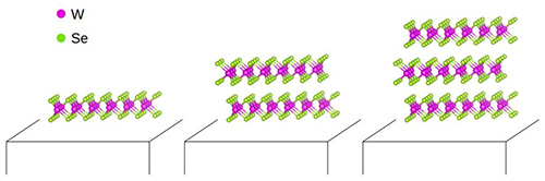
The general formula of TMD is MX2, where M is a transition element and X is a chalcogene. Those two elements form a MX2 basic layer, where M atoms are sandwiched between two covalently-bonded planes of chalcogenes. The three-dimensional (3D)-solid is obtained by stacking these X-M-X sheets, only weakly bonded by van der Waals interactions, conferring to TMD a very pronounced 2D-character (figure 1).
In bulk TMD, due to the hybridization of the orbitals pointing out from the MX2-planes, electrons can « jump » from one layer to the other and band dispersions can be observed in this z-direction normal to the sheet plane. In other words, the energy of the electrons depends on the wave vector component along the z-direction, kz. On the other hand, no kz-dispersion is expected at the single-layer limit since electrons are confined in the MX2-plane.
How does this crossover from a 2D to a 3D electronic structure take place?
Scientific approach
Using angle-resolved photoemission spectroscopy on a synchrotron radiation source at the CASSIOPEE beamline of SOLEIL, the scientists precisely addressed the two-dimensional to three-dimensional crossover of the electronic band structure in large area epitaxial WSe2 thin films.
The samples were grown by Molecular Beam Epitaxy (MBE) on graphene/SiC(0001). Samples of 2, 3 and 6-7 layers of WSe2 were studied. For each sample, the band dispersion along kz, corresponding to the Γ-A direction of the reciprocal space (See panel (a) of figure 2) was measured.
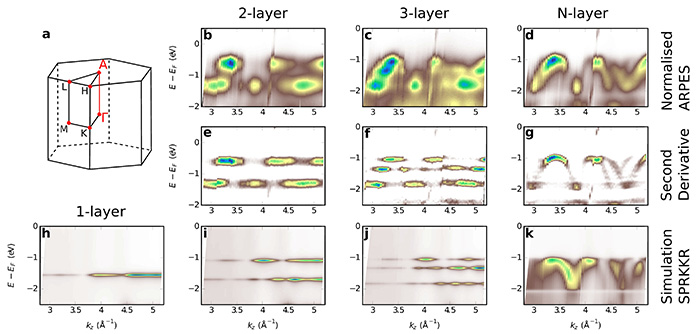
The (b-d) panels of figure 2 show the raw data for the three samples. For the 2-layer sample, the two bands which are the closest to the Fermi level clearly have a discontinuous kz-dispersion, consisting in linear segments (no kz-dependence of the electron energy) corresponding to kz-ranges where these bands appear. The same phenomenon is observable on the 3-layer sample with instead three bands appearing and disappearing. Nevertheless, the bright segments are shorter in kz and more numerous for each band. They start to draw the band oscillations that we clearly see in the (6-7)-layer case, where the observed dispersion compares well with previously measured data on bulk-WSe2. This is more visible on the second derivative images (panels (e-g)). Panels (h-k) display calculations done with the SPRKKR code which solves the Dirac equation using multiple scattering and Green’s functions. They reproduce very well the experimental results.
Summary
In a single layer TMD, the electrons are confined within the layer and form a unique discrete (at a fixed energy) energy state. As the number of layers increases, the electrons can populate more and more discrete states at different energies which eventually form the continuous 3D band dispersion of the bulk crystal.
This work is part of the PhD of Raphaël Salazar, done à SOLEIL and funded by the French Agency for Research (CORNFLAKE project , ANR-18-CE24-0015-01).