Study of an infrared camera using operando photoemission on ANTARES beamline
Nanocrystals are semiconductor nanoparticles. By choosing the right materials, it is possible to design nanocrystals photosensitive to infrared (IR) light, which can then be used as "active pixels" in IR detectors. In recent years, significant progress has been made in switching the design of device from a single active pixel to a full camera.
Scientists at INSP (Sorbonne University, CNRS), in collaboration with the SME New Imaging Technologies, have developed an IR camera whose active layer consists of HgTe (mercury telluride) nanocrystals. Manufacturing a sensor based on these nanocrystals is less costly and uses fewer toxic materials than conventional devices. The ANTARES beamline has enabled the scientists to reveal the energy profile of this sensor's surface during operation.
To date devices operating in the infrared present a prohibitive prize (up to 100 k€ for a camera) to be used in mass market application such as assistance to night driving. Part of this problem comes from the growth cost of the involved semiconductor. This is why there is a very strong effort to make emerge new infrared active materials. Among the candidates, narrow band gap* colloidal nanoparticles of HgTe have gained considerable maturity over the past decade. By careful choosing their size (around 6 nm, see Figure 1a) it is possible to make them in the short-wave infrared (Figure 1b). A team from INSP together with the SME New imaging Technologies has succeeded in coupling a film of such an infrared active material to a CMOS read out integrated circuit to design a full imaging setup. An example of the obtained image is shown as Figure 1c.
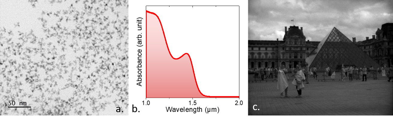
a. Electronic microscopy image of HgTe nanocrystals
b. Absorption spectra of these HgTe nanocrystals, showing the material's ability to absorb photons with wavelengths between 1 and 1.7 µm.
c. Infrared image of the Louvre Museum acquired with the camera made of HgTe nanocrystals.
So far, the design of devices based on such new materials relies on measurements of the physical properties of the pristine material, assuming that its electronic structure will remain mostly unchanged once the material is integrated -for example- into a camera. A more detailed description should be based on in situ measurements in the device and possibly while the device is in operation, to also account for the effect of applied electric fields. However, achieving such measurements requires properly suitable tool.
Here, the electron photoemission microscope implemented on the ANTARES beamline was used to probe the energy landscape of the sensor within the device. The soft X-ray beam (wavelengths of the order of a few nm) were used as a local probe of the sensor's electrical potential, see a schematic of the experiment in figure 2a. The analyzer (the half-sphere in Fig. 2a) then measures the speed of the emitted electrons, from which the force binding these electrons to the atoms constituting the material can be deduced. This time the team further used the high resolution of the beamline not only to probe the potential but also the vectorial distribution of the electric field (figure 2b) which can be quite complex on the surface of the read-out circuit where biases are applied with 2D checkerboard distribution. Access to such measurements can then be used to better understand the active area of the component, or to model the transport of electrical charges over the sensor surface.
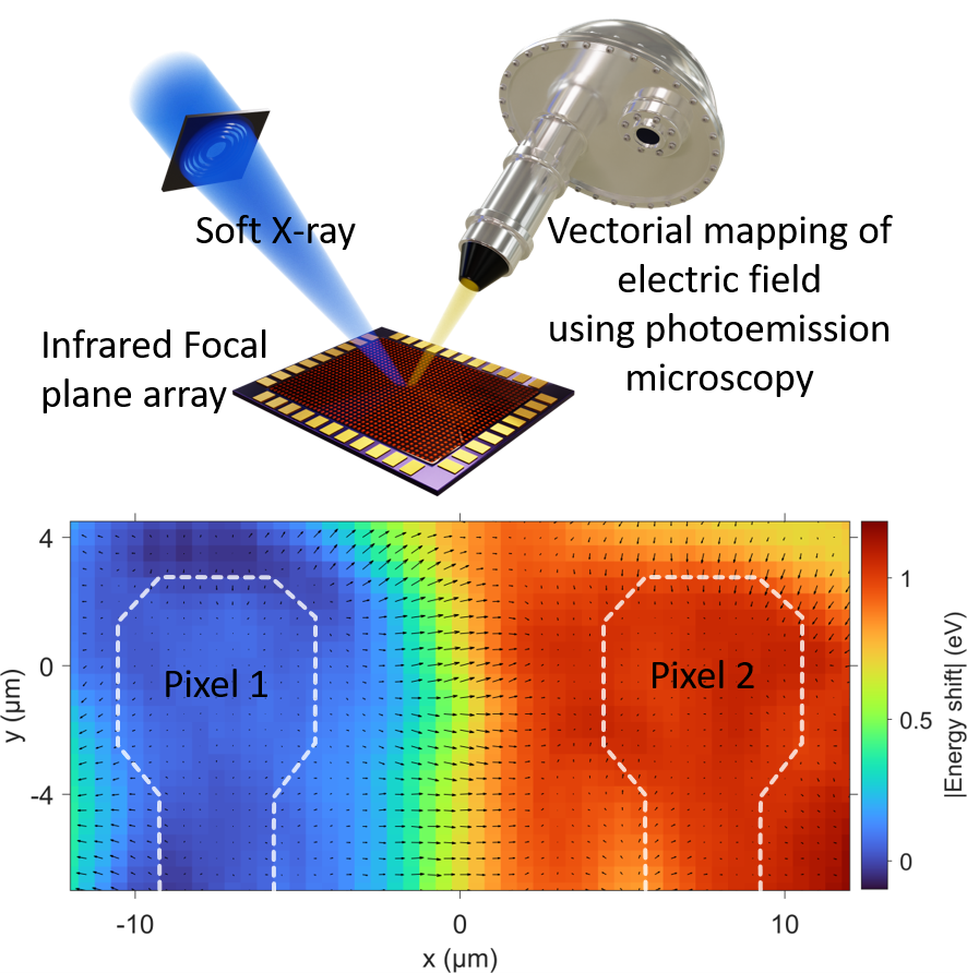
a. Schematic of the experiment conducted on ANTARES beamline. The X-ray beam is focus with a Fresnel lens on the sensor which active layer is made of HgTe nanocrystals. The energy of the electrons emitted by the sensor illuminated by X-rays is then measured using an electron analyzer. Repeating the same experiment while the beam is scanned over the entire surface of the sample enables to map the device energy landscape.
b. Distribution of the electric field between the pixels, delimited by the white dotted lines. The arrows indicate the direction of the electric field, and their length corresponds to the field intensity.
The method, quite general, is not limited to the case of infrared imager: it can be applied to a wider range of materials and devices. INSP and ANTARES beamline will now pursue this effort in the framework of a new ANR project, “E-map”.
The article describing these results appears on the cover of the August 2023 issue of the ACS Applied Electronic Materials Journal (figure 3).

* bandgap: corresponds to the energy an electron in the material must acquire to become free to circulate - in the case of a semiconductor, this is the energy it must acquire to pass from the insulating state to the conducting state. This energy can be supplied by light: for HgTe, by infrared light.