Silicene ribbons mounted on gold …
Shortly after the discovery of the remarkable properties of graphene, researchers from French, Swiss, American and Moroccan laboratories have undertaken studies to see if silicon, the closest element to carbon, could adopt a structure similar to graphene. Their latest findings, published recently in APL [1], show for the first time that it is possible to grow silicene on a gold substrate. Characterization of the nanoribbons of silicene obtained was carried out using high resolution photoemission spectroscopy on the TEMPO beamline.
Silicon, placed just below carbon in the periodic table of elements, has an outer electronic structure similar to that of carbon and could therefore have a similar range of allotropes.
A few years ago, the authors of this study showed that silicon, when deposited on silver metallic substrates, could adopt the atomic structure of silicene, analogous to graphene, and organize itself either into 1.6 nm-wide ribbons or into two-dimensional layers [2].
A more recent study done in the ISMO-Orsay laboratory and published in APL [1], shows for the first time that it is also possible to grow nanoribbons of silicon on a gold surface (110) and that these have an atomic structure analogous to the silicene grown on silver.
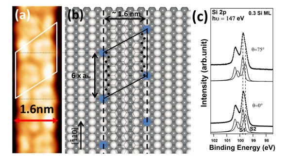
Figure 1 shows an image, obtained by scanning tunneling microscopy, of a 1.6 nm-wide silicon nanowire, which can be explained as an internal honeycomb-like structure covering four rows of gold surface atoms (Fig. 1b). The Si2p core levels (Fig.1c), measured on the TEMPO beamline at SOLEIL, then show that the silicon has only two chemical environments, as previously observed with silicon ribbons on silver. The first corresponds to the silicon atoms located at the wire edge and the second corresponds to the atoms inside the wire.
This study therefore shows that silicene can be grown on substrates other than silver. A new challenge is now to grow the silicene on insulating substrates, which would lead to the manufacture of silicene- based electronic devices.