Photoactive clay nanotubes for hydrogen production
Photocatalysis1 is considered one of the cheapest and most efficient technology for solving the problem of global energy shortage. One of the challenges is to find the right photoactive material for an efficient process. Clay nanotubes are attracting renewed interest thanks to their unique physical properties and the possibility to dope their structure to enhance charge-carriers separation into their structure. Through an international consortium, researchers from Laboratoire de Physique des Solides (CNRS/UPSaclay) have demonstrated a step‐forward on photocatalytic H2 production achieved through atomic doping of clay nanotubes.
How fundamental chemical and/or physical principles differ when photocatalytic systems are restricted to nanoscale dimensions? The rise of nanoscience and nanotechnology offers an ideal playground for exploring these concepts from nanotubes to more complex 3D porous architectures. In particular, synthetic imogolite clay nanotubes (INTs) with chemical formula (OH)3Al2O3Ge(OH) appear as promising photocatalytic materials. The scientific interest inthese nanotubes stems from ab initio calculations that predict atypical spatial separation of the valence (VB) and conduction band2 (CB) edges across the nanotube walls, which would promote redox reactions at separated locations. However, their large band gaps2 have inhibited their use as photocatalysts.
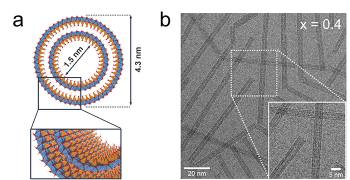
The first step toward using these nanotubes in photocatalysis and exploiting the polarization-promoted charge separation across their walls is to reduce their band gap. An international consortium led by researchers from Laboratoire de Physique des Solides investigated the potential of synthetic double-walled imogolite nanotubes (Figure 1a) for photocatalytic applications. Substitution of Ge precursor3 by Ti precursors (doping) is carried out to transform pristine imogolite from non-photoactive material to a photocatalyst efficient for H2 generation. Various Ti/Ge samples are prepared by changing the initial precursor ratio x = [Ti]/([Ge]+[Ti]). Morphological investigations by X-ray scattering and conventional cryo transmission electron microscopy (cryo-TEM) reveal the preservation of the nanotube shape up to x = 0.4 (Figure 1b).
(a) Schematic view of a double-walled imogolite nanotube (DWINT) structure with Al, Ge and O atoms represented in blue, orange and red, respectively.
(b) cryo-TEM images of Ti/Ge samples synthesized at a doping ratio x = 0.4.
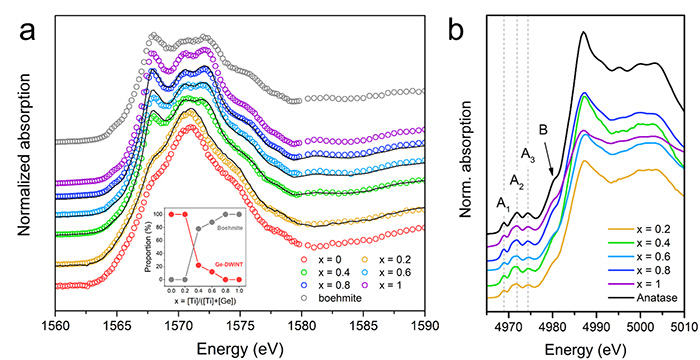
Understanding the local structural modifications of the nanotubes is essential for further investigation of the photoinduced properties of these doped-nanostructures. To confirm the doping modification, a multiscale characterization was performed by combining different X-ray spectroscopies and in particular X-ray absorption near edge spectroscopy (XANES) on LUCIA beamline. XANES at the Aluminium K-edge reveal a large absorption band located at 1571 eV, characteristic of Al in an octahedral configuration (Figure 2a). A lower energy resonance appears at 1567 eV with increasing the precursor ratio, which is related to the presence of a by-product Aluminium boehmite (aluminium oxyhydroxyde AlO(OH)) phase as demonstrated by linear combination fitting of XANES spectra. XANES spectra at the Ti K-edge present the characteristic pre-edge modes attributed to 1s to 3d dipolar transitions of Ti4+ in octahedral configuration. These results indicate that Ti atoms seem to replace preferentially Aluminium atoms.
(a) Al K-edge. The black curves correspond to the linear combination fitting using x = 0 and x = 1 as references. The resulting proportion is displayed in the inset.
(b) Ti K-edge.
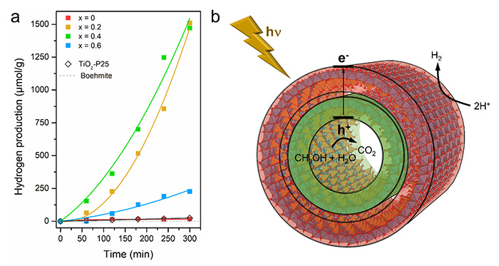
The incorporation of Ti in the nanotubes modifies its band structure sufficiently to confer them unique photocatalytic properties. The photocatalytic efficiency reveals a high hydrogen production of ~1500 µmol g-1 for noble metal-free photocatalyst, 65-fold higher than the commercial TiO2-P25 (Figure 3a) in similar conditions of water splitting with an electron donor. This is correlated to a lowering of the recombination rate of photogenerated charge carrier for the most active structures. Instead of using a metal co-catalyst as a reduction site and electron collector, the natural polarization of Ti-doped nanotubes facilitates the photogenerated charge separation, making the reduction and oxidation sites spatially separated, as illustrated in Figure 3b. The photogenerated charges induce dissociative adsorption of methanol, used as electron donor, and hole scavenging, which is followed by hydrogen ion release. The reduction leading to the formation of an H2 molecule is expected to be localized in the outer surface of the nanotubes, while the oxidation takes place in the nanotubes (Figure 3b).
(a) Hydrogen evolution reaction under solar-light irradiation for Ge-DWINT and Ti/Ge samples with different ratio with comparison with internal standards.
(b) Schematic illustration of the proposed H2 production mechanism, pointing out the general steps involving electron/hole charge separation/reaction pathways.
These results confirm the theoretical predictions regarding the potential of modified imogolite nanotubes as photoactive nanoreactors and pave the way for investigating and exploiting their polarization properties for energy applications.
-------------------------------------------
1 - Photocatalysis is a phenomenon in which a "photocatalyst" material accelerates the speed of a chemical reaction under the action of light, natural or artificial.
2 – Conduction/valence band & band gap: in solids, the energy of the electrons can have any value within certain intervals, called “allowed bands”, separated by “forbidden bands”. In an insulator, a wide band gap separates the valence band - in which electrons do not participate in electrical conduction - and the (electrical) conduction band. In a conductor (metal), valence and conduction bands overlap: electrons from the valence band can pass into the conduction band and circulate in the solid. In a semiconductor, the band gap is narrow: electrons from the valence band can pass into the conduction band if they are given a little energy (electricity, light). It is also possible to control this transition to the conduction band (and hence the material's conductivity) by doping.
3 - Precursor: molecule composing the nanotube; several precursors, containing different ratios of Ge and Ti atoms, were tested in this study.


