Optoelectronics: Benefit of semiconductor/ferroelectric hybrid material
Semiconductor nanocrystals are promising building block for optoelectronics. Over the past three decades, large progresses have been obtained on their synthesis to achieve size and shape control and expand the library of material. In spite of this breakthrough, the modulation of their doping (i.e., the fine tuning between their metallic and insulating behavior through generation of free electric charge carriers) remains a bottleneck for their integration.
Scientists at INSP and C2N, in collaboration with the ANTARES beamline, have explored a generic method where remote doping is achieved by coupling the nanocrystal layers with patterned ferroelectric* domains.
Thanks to their cost-effective growth and their broad spectral tunability (i.e. possibility to change their color including beyond the visible range), narrow band gap nanocrystals (i.e. compatible with an absorption wavelength in the infrared) appear very promising for infrared optoelectronics, in particular for sensing where current technologies cost prevents their mass market use. Beyond the band gap design, the modulation of the electrical properties, via a doping strategy, also plays a central role. For "traditional" semiconductors, doping can be done by adding small quantities of impurities, notably. But, in nanocrystals, self-purifying effect prevent introduction of extrinsic impurities or leads to electrically inactive dopant - i.e. charges that do not carry electricity. Because of this difficulty, method relying on transistor have been developed. Dual gate device can be used to shape the carrier density landscape and form pn junction, a central building block of optoelectronic used for LED and detector. Though the concept has been developed, the introduction of extra electrode also tends to bring additional noise device, thus asking for passive (without applying an external bias) strategies to generate pn junction.
Here, the possibility to replace the gate by ferroelectric domains has been explored.
A consortium made of C2N for the ferroelectric growth, INSP for the nanocrystal growth and ANTARES beamline to conduct nanoimaging, has demonstrated how ferroelectric materials can be used to create a pn junction in nanocrystal semiconductor film. The teams have used PbZrxTi1−xO3 (PZT) as ferroelectric material, then using Piezoresponse Force Microscopy (PFM) they have defined two domains of opposite polarization. Finally, the device was covered with an infrared nanocrystal film that is used to absorb light, see Figure 1b. To bring direct demonstration of the coupling between the ferroelectric and the nanocrystal electronic structure, the nanobeam of ANTARES beamline has been used, see Figure 1a.
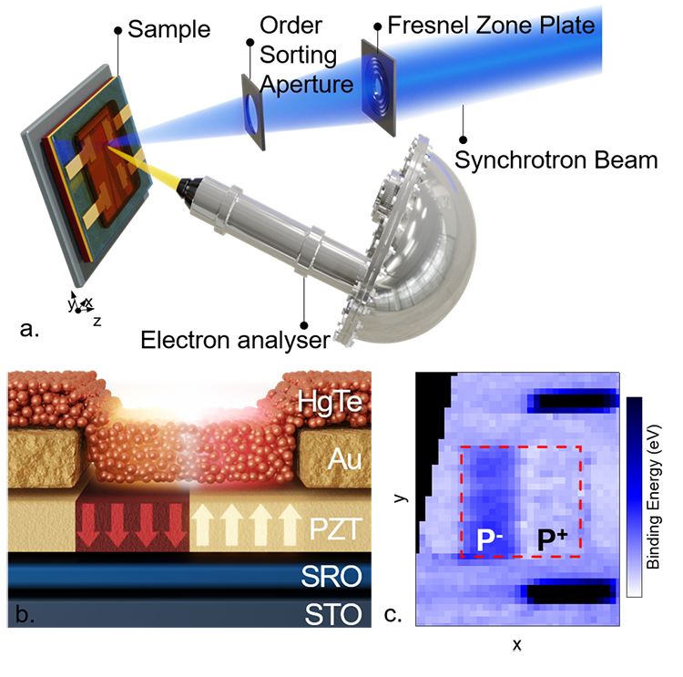
This nanobeam allowed them to image the binding energy shift of the nanocrystals when in contact with the two ferroelectric domains exhibiting opposite polarization. This energy shift can reach 115 meV which corresponds to ≈1/4 of the optical band gap, see Figure 1c.
Finally, scientists have performed electrical measurements and confirm that the configuration with two opposite polarizations indeed leads to the formation of a diode presenting the characteristic rectifying current-voltage behavior: an asymmetric IV curve in which the device allows the current flowing in one direction while restricting the flow in the opposite direction.
The benefit of this strategy is the possibility to generalize it to other configurations and materials since it does not require any modification of the light absorbing layer. Now future work will have to focus on strategies to couple this surface effect with strong absorption required for light sensors.
* Ferroelectric materials show a spontaneous electrical polarization which can be inverted by applying a simple electric field. This property makes them very interesting candidates for a new generation of electronic devices less energy-consuming and presenting a high-speed reading and a high-density storage capacity.