Molecular nanowires in miniaturized electronic devices : The contribution of the GIWAXS technique developed on the SIRIUS beamline
Molecular electronics enables the development of breakthrough applications for photovoltaic panels, lighting, displays, sensors, flexible electronics, etc. It aims to offer an alternative to conventional silicon circuits, which have reached their miniaturization limits. Its principle: to use molecular "Lego® " which self-assemble into domains to transport electrical charges — the size of electronic components is thus drastically reduced.
To monitor the synthesis of such devices at the nanometric scale and to characterize them, grazing incidence wide angle X-ray scattering (GIWAXS), implemented on the SIRIUS beamline, appears to be a reference analytical technique.
Electronic devices are traditionally fabricated via a multi-step sequence of complex and costly techniques during which electronic circuits are gradually created on a wafer made of pure semiconductor material. The limits in terms of minimum size reached by this top-down approach can be overcome by a bottom-up approach, as used in molecular electronics, which consists in building components molecule by molecule. Supramolecular electronics is the link between molecular electronics and etched devices. In particular, it allows the interconnection of nano- or microelectronic circuit elements using supramolecular polymers consisting of a long chain of self-assembled organic molecules. These so-called "1D" (one-dimensional) polymers are synthesized by in situ electropolymerization between microelectrodes to produce extremely thin nanowires. The process must be very precisely controlled, as the efficiency of the whole device depends not only on the structure of the molecular building blocks assembled in the nanowires, but also on their orientation and alignment over distances of the order of a micrometer.
But no standard analysis techniques allow the structural and full orientation characteristics of these nanowires in electronic circuits to be accessed at this scale.
All the information captured in one shot
X-ray scattering techniques can give access to the organization of materials down to the atomic scale. However, studying only a few nanowires placed in an electronic circuit is complex, on the one hand because of the very small amount of material and therefore the very low intensity of the measured signal, and on the other hand because of the device geometry: in this work, the microelectrodes obstruct the trajectory of the X-ray beam and hinder the measurement.
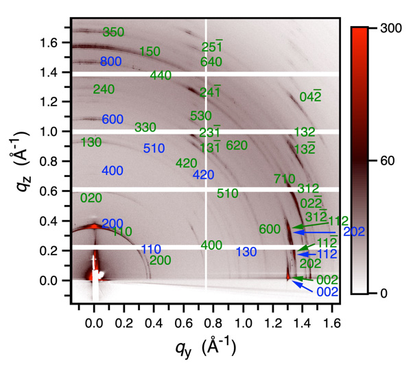
To overcome these limitations, researchers from Charles Sadron Institute (Strasbourg), Institute of Physics and Chemistry of Materials (Strasbourg) and SIRIUS beamline at SOLEIL have developed an experimental set-up allowing GIWAXS analysis of the entire morphology of organic electronic circuits: here, nanowires made of triarylamine (TAA) – a family of molecules with excellent electronic and photonic semiconducting properties – are assembled directly between the electrodes by a supramolecular electropolymerization process. The scientists were thus able, in a single shot, to determine the structure of the nanowires interconnecting the microelectrodes, as well as their orientational order parameters in 3D (showing that the nanowires all grow parallel to the plane of the substrate) and in 2D (in the plane, the nanowires align perpendicular to the microelectrodes). This alignment occurs with a coherence length of more than 100 nm, representing more than 200 molecules along the long axis of the nanowires.
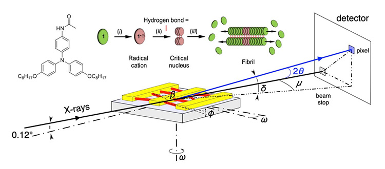
Top left: Molecular structure of a TAA1 molecule.
Top center: supramolecular polymerization mechanism of TAA1 by an oxidation/nucleation/growth process.
Bottom: Experimental setup for GIWAXS measurements on SIRIUS; the TAA nanowires (in red) elongate in situ between the electrodes, shown in yellow (width 10 µm; height 100 nm; spaced away by 10 µm). The angles ∅ and β define the disorientation of a nanowire long axis with respect to the substrate plane and to the normal to the electrodes, respectively.
These results provide information inaccessible by other analysis techniques reported in the literature, such as the full set of crystal lattice parameters and molecular organization modeling, even though the nanowires can only be probed in one orientation of the miniature electronic device, due to the beam obstruction by the microelectrodes.
All the parameters determined through these measurements are of crucial importance to investigate the structure-function relationships in the molecular electronic devices.
This work demonstrates the great potential of the GIWAXS technique as a reference method for the comprehensive characterization of supramolecular nanowires and other self-assemblies embedded in complex device geometries.