Infrared electroluminescence from nanocrystals
While energy consumption becomes a major challenge, achieving efficient light source become of utmost interest. This is not only true in the visible spectral range but also in the infrared. Currently the range from 1.5 to 4 µm lack of efficient source, while several applications such as gas spectroscopy, airfield lightning or autonomous vehicle requires such source at low cost. Here, researcher have demonstrated the design of a light emitting diode with emission in the 2 to 2.3 µm range using colloidal nanoparticle as building block.
Nanocrystals are semiconductor nanoparticles which color can easily be tuned through their size. They have initially been designed to emit light in the visible range and they are now used in display as green and red light source. However, the potential of nanocrystal is not limited to wide band gap material and it is also possible to achieve tunable optical feature in the infrared using material such as PbS or HgTe. Such nanoparticles have been integrated for the design of solar cell or image sensors for example -in these devices, nanoparticles absorb IR light. Far less efforts have been dedicated to the emission properties of these nanoparticles in the infrared range, while they appear to be bright light source.
The field of infrared source is mostly dominated by semi-conductors like InGaAs, InSb ou HgCdTe, obtained using epitaxy process. In the telecom range -around 1.5 µm- fast, high-power source have been obtained using quantum well structure. Similarly, above 4 µm, quantum cascade lasers now achieve high brightness. It remains that there is a technological gap between 1.5 and 4 µm where only a few technologies are available. A consortium of researcher (Sorbonne Université - INSP, ENSTA - LOA, ESPCI, C2N, Synchrotron SOLEIL and ONERA) have design the first nanocrystal-based light emitting diode (LED) with operation above 2 µm, see figure 1.
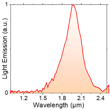
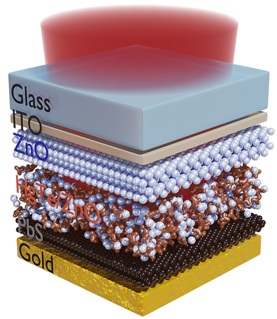
To design such a LED they design a stack of layer, where the light emitting material (HgTe) is sandwiched between a ZnO and a PbS which are respectively in charge of electron and hole conduction, see figure 2. The device achieves an external quantum efficiency of 0.3%, comparable with state-of-the-art epitaxially-grown LEDs in the similar wavelength. A low turn-on voltage of 0.6 eV (≈EG/e) and a bright radiance up to 3 W.Sr-1m-2 are also obtained.
The operation mechanisms of the device, particularly the role of ZnO within the HgTe:ZnO layer, are elucidated with three approaches: (1) electrical transport, (2) transient reflectivity spectroscopy, and (3) time-resolved X-ray photoemission that has been conducted on the TEMPO beamline of SOLEIL. The results indicate that, in the HgTe:ZnO layer, the HgTe NCs govern the transport while the ZnO NCs content tunes the majority carrier hence the charge balance in the device, which is essential for high performances.
Future work will have to focus on improving the device performances which can be achieved by a better engineering of the light extraction and of the electronic band alignment of the components, on which the transfer of electrical charges in the device depends.