Future of organic thin film electronics: the crucial role of surface chemistry
The next generation of wearable and stretchable electronics will rely on the development of low-cost, high-performance electronics using organic semiconductor films. Such development requires to understand how surface chemistry affects the growth of these organic semiconductor films.
Researchers at the University of Ottawa characterized thin films of bis(pentafluorophenoxy) silicon phthalocyanine (F10-SiPc), a promising organic semiconductor, on a range of different surfaces to understand how surface chemistry affects resulting film and device properties. Grazing-Incidence Wide-Angle X-ray Scattering (GIWAXS) at the SIRIUS beamline was used to study molecular orientation of F10-SiPc within the films.
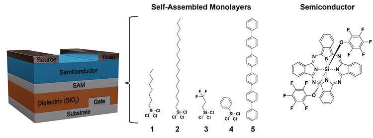
Researchers at the University of Ottawa are optimizing organic thin-film transistors* (OTFTs) based on F10-SiPc. By modifying the substrate, the texture of F10-SiPc semiconductor film can be controlled by its interactions with the surface of the substrate on which it is deposited. These interactions depend on either the terminal chemical group of the templating molecules of the substrate, or on the surface energy which dictates the attraction between molecules and the surface. The molecules used to generate functional surfaces in this work are silanes, which are linear molecules that form a bond with the surface (molecules 1 to 4 in the figure 1), and para-sexiphenyl (p-6P ; molecule 5 in the figure 1), which is evaporated as an ultra-thin layer that serves as a template for the organic semiconductor (Figure 1).
While previous studies have optimized SiPc-based OTFTs using silanes, the effect of different functional surfaces on the texture of films and resulting device performance is not well understood for these materials. This work explores functional surfaces with silanes of different lengths and terminal groups, as well as the use of p-6P, and their impact on the growth and texture of F10-SiPc films, the crystallinity of these films, and the feature sizes of crystals in the films.
GIWAXS Measurements on SIRIUS
At the SIRIUS beamline, Grazing-Incidence Wide-Angle X-ray Scattering (GIWAXS) was performed on films of F10-SiPc evaporated onto five different templating layers deposited on silicon oxide wafers. Samples were prepared by modifying the substrate with the templating layer, followed by evaporation of F10-SiPc by physical vapor deposition.
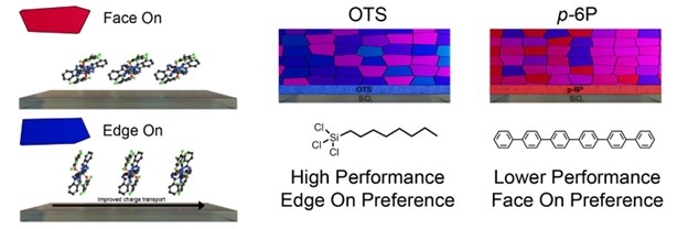
Understanding the orientation of F10-SiPc in the film is important when optimizing the performance of OTFTs. GIWAXS identified whether F10-SiPc molecules deposited relative to the substrate surface in a “face-on” orientation, where the conjugated part of the F10-SiPc is parallel to the substrate, or in an “edge-on” orientation, where the conjugated macrocycle is perpendicular to the substrate. In typical OTFTs charges hop between the macrocycles meaning an edge-on orientation is desirable to improve device performance.
Films evaporated on n-octyltrichlorosilane (OTS) yielded the best OTFTs due to F10-SiPc having both the largest crystallite size and significant regions with edge-on orientation. F10-SiPc on p-6P yielded interesting results, given that F10-SiPc molecules had a mix of orientations, neither being edge-on. This is different from other phthalocyanines which typically yield edge-on films. We suggest the bulky axial substituents of F10-SiPc play a significant role in determining the molecular orientation (Figure 2).
This study demonstrated the importance of considering both semiconductor molecular design and surface functionalization when evaluating how surface chemistry can influence the growth of evaporated films of F10-SiPcs, including their texture and properties in organic electronic devices. These results will inform the design of new SiPcs and functional surfaces to optimize SiPc-based OTFTs.
* A thin-film transistor is made by depositing thin layers of materials (semiconductors, metals or insulators) on a substrate. These layers are generally a few nanometers thick.