The first "made-in-SOLEIL" hybrid pixel modules
To meet the needs of pump-probe-probe time-resolved X-ray diffraction experiments, such as those carried out on CRISTAL beamline, the Synchrotron SOLEIL Detectors group launched an R&D project in 2017. Carried out in collaboration with the AGH-UST faculty of Krakow (Poland), which supplied the integrated microelectronic circuits allowing readout and processing of the signal, this project consisted of designing a new fast detector of photon counting type and time resolved.
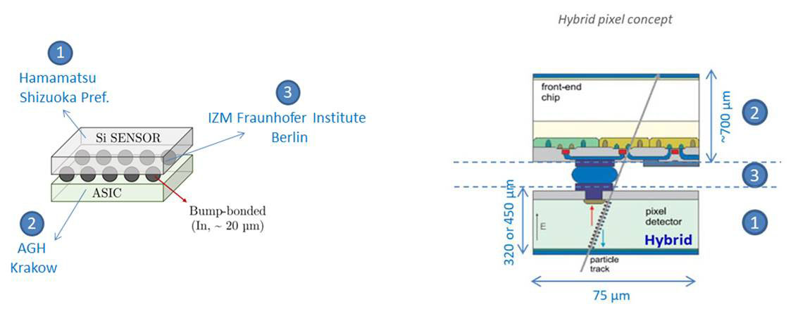
This detector uses the well-known hybrid pixel technology. The detector is composed of several pixel matrix modules. Each pixel is 75 µm square. Hybrid pixels, which are high-tech objects, have the particularity of being composed of two interconnected micro-electronic circuits, stacked like a sandwich (see illustration of the concept in Figure 1).
The very first hybrid pixel modules were provided by AGH-UST faculty collaborators and implemented on a 2 × 2 cm2 [Reference 1] square prototype detector. The Synchrotron SOLEIL Detectors group also needed to design and produce its own hybrid pixel modules, of different size and geometry, to meet SOLEIL's specific needs appropriately.
To achieve the final result, a multitude of complex steps must be accomplished:
1. A sensitive layer for photon detection
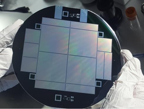
This involves designing the layer that is sensitive to photon radiation. To optimise manufacturing costs, we have designed pixel matrices of several geometries and sizes on the same silicon wafer, as shown in the photograph Figure 2. The pixels are of the “P-on-N” type, which means that the collection of charges, created by the interaction of photons, is done by diffusion and derives of the holes in the N-doped silicon to the P-type electrode (pixel) through the application of a high voltage. Hamamatsu (Japan), a company specialised in silicon wafers for this type of custom application, finalised the manufacturing files according to our specifications and our technical exchanges. Once produced and inspected in a clean room at SOLEIL, the silicon wafers, which potentially contain several future detectors, were sent to the IZM-Fraunhofer Institute (Germany), a specialist in the manufacture of hybrid pixel modules.
2. Signal readout and processing layer
This involves designing the layer of microelectronic chips, also called ASICs, which read out and process the signal collected from the previous layer. This design was made by the microelectronics group of the AGH faculty in Krakow (Poland). The production was carried out by a confidential and appropriate founder, with a very precise submicronic technological choice. As in step 1, these reading chips are also in the form of a large wafer of approximately one hundred chips. After testing and selecting the best chips (rated A, B, C, and D), this large wafer was also sent to the IZM-Fraunhofer Institute (Germany).
3. Interconnection of hybrid pixels (“Bump bonding” step)
During this crucial and delicate step, the following is implemented:
- Each chip of the detection layer of the first wafer is carefully cut out.
- The selected chips from the second wafer are cut out.
- The metallization layers necessary to connect the chips are made.
- The indium microballs are placed on one of the two layers.
- The chips of the future sandwich are very precisely aligned one above the other.
- Pressure is applied to reseal and gently heat to connect the sandwich to form the hybrid pixel modules.
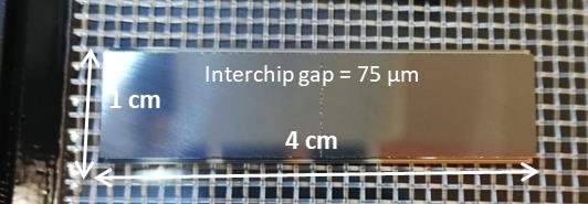
This technique is called “bump bonding” interconnection. In Figure 3, a finalised rectangular module of 65,536 hybrid pixels is illustrated. This module is composed of two readout ASICs and a single silicon sensor (no dead area for detection). Each manufactured module is then inspected by X-ray to ensure that all 65,536 connections are present (no missing balls, no cracking, etc.). It is important to know that, at this stage, it is not uncommon to break and damage a large number of modules. Finally, once the modules have been manufactured, they are inspected in a clean room at SOLEIL before transferring them definitively to their electronic board.
4. Interconnection of hybrid pixel modules on their electronic board ("wire bonding" step)
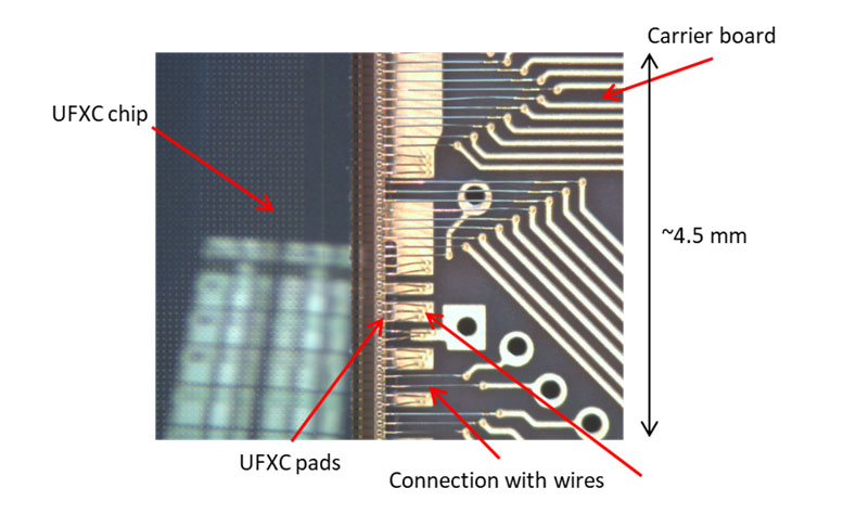
The hybrid pixel modules are then transferred definitively to their electronic board (complex printed circuit board), where they are carefully connected using the "wire bonding" technique. The connection is made pad-to-pad by gold or aluminium wires 18 or 25 µm in diameter. Figure 4 shows a photo of a zoomed part of the hybrid pixel module with the "wire bonding" wires. Once again, several modules could be irreversibly damaged during this delicate step.
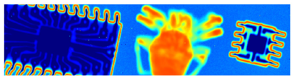
5. Validation tests of complete assemblies with X-rays
The final step in the process is to test the functionality and performance of our manufactured hybrid pixel modules. To do so, they are tested using the X-ray generator of the Detectors group. Figure 5 illustrates an example of an image obtained with a photons beam of energy E = 14 keV. In this figure, the module is fully functional, the pixels have been calibrated and the rate of dead pixels is very low of the order of 0.04%, which is a very good value for this type of detector.
Other modules are currently undergoing validation tests and will soon be assembled with their mechanics and acquisition system to make a complete detector ready for use.
In summary, the Synchrotron SOLEIL Detectors group has successfully produced its very first hybrid pixel modules. These modules are complex, high-tech objects, which involved five companies and two research laboratories, excluding SOLEIL, for a design, manufacturing and validation test period ranging from 14 to 18 months (outside the context of the COVID epidemic).
Note: The first experimental results were obtained at the end of 2019 [Reference 2] on CRISTAL beamline with the first hybrid pixel modules from the AGH faculty. The new rectangular 'made-in-Soleil' modules were tested in February 2021 on ODE beamline; other beamline experiments will be planned soon with this particular elongated geometry. In parallel, larger hybrid modules with 8 ASICs have also been manufactured and will be tested soon.