Deformation of nanocrystals under irradiation
Unlike soft condensed matter, crystalline solids are not particularly subject to phase change effects under illumination. With the emergence of nanometric size solids, this resistance to radiation has been questioned, as demonstrated by scientists at the Institute of Electronics, Microelectronics and Nanotechnology (IEMN) and ANTARES beamline, who analysed semiconductor nanocrystals with a so-called core-shell structure.
Semiconductor nanocrystals are nanometric particles from 2 to 10 nanometres in size, whose physical properties are dominated by quantum confinement effects. Their most striking property is related to their light emission at a wavelength defined by their size. Such inorganic crystalline materials, created by a low-cost chemical synthesis process, decay much more slowly than classic organic fluorophores, and are often used as biological labels. In recent times, they have also been incorporated in optoelectronic components such as LEDs and solar cells.
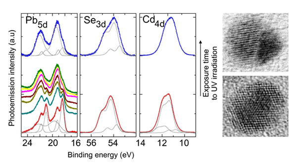
Their fluorescence efficiency has been greatly improved with the creation of a shell consisting of a different semiconductor material, which passivates the core of the nanocrystal and increases the probability of light emission. But this layer can also modify the electronic structure of the nanocrystal. Synchrotron radiation is an appropriate technique to probe the electronic properties of semiconductor heterostructures and to determine their chemical composition. When applied to nanocrystals with a core consisting of lead selenide (PbSe) and a shell of cadmium selenide (CdSe), this technique has revealed an electronic and chemical change in the nanocrystals under high-energy UV radiation (90 eV). This change corresponds to a phase transition during which the nanocrystal is transformed from a core-shell structure to a Janus structure formed by two hemispheres: one of lead selenide and the other of cadmium selenide.
The deformation of the nanocrystal comes from a minimisation of the interfacial energy between the two materials under the effect of the radiation. This study shows that electromagnetic radiation can be used to transform materials of nanometric size to obtain objects that cannot be manufactured via conventional chemical synthesis or growth methods.