Bottom-up nanofabrication enabled by the layering of block copolymer films
Block copolymers (BCPs) are ubiquitous in our daily lives and are found in products such as adhesive tapes and cosmetics. These macromolecules are produced by joining two chemically-distinct polymer chains (the “blocks”), that may be incompatible (like oil and water). The segregation of these “blocks” produces complex structures at the nanoscale. BCPs can thus be used for nanofabrication with flagship applications in lithography and optics. Nevertheless, the range of geometrical features is limited, and the layering of BCP layers is foreseen to enrich the span of structures.
Since its advent in the 1960s, the semiconductor industry has witnessed the doubling of integrated circuit (IC) transistor density biannually. Colloquially referred to as Moore's law, silicon transistor dimensional scaling has been forbiddingly aggressive – from 10 μm in 1971 to 14 nm today. The miniaturization of IC features serves to provide us with faster, smaller and cheaper electronic devices. However, the evolution of consumer electronics with the development of the Internet-of-Things, in conjunction with the narrowing window of optical lithography capabilities, has placed the semiconductor industry at a crossroads. New materials and processes are needed and complementary “top-down” (component made by "cutting" a material) and “bottom-up” (component made by assembly of sub-units) patterning methodologies are explored to continue Moore's law.
Among them, BCP self-assembly in thin film is an elegant method to generate nanoscale features with tunable geometrical configurations. By combining directed assembly and hybridization methods, “bottom-up” nano-manufacturing have been applied for the design of functional structures with flagship applications in lithography and optics (bottom-up approaches use chemical or physical forces to spontaneously self-assemble, organize atoms, molecules, or nanoscale building blocks into larger ordered structures).
Nevertheless, the range of geometrical configurations is limited by the accessible morphologies inherent to the energy minimization process involved in BCP self-assembly. Layering of nanostructured BCP thin films has been recently proposed in order to enrich the span of nanostructures.
In this work, the scientists further exploited the layer-by-layer method for the generation of nano-mesh arrays using nanostructured BCP films. In particular, they leveraged a subtle combination of chemical and topographical fields in order to demonstrate design rules for the controlled registration of a BCP layer on top of an underneath one by the precise tuning of the interfacial chemical field between the two layers. They demonstrated that the change of the interfacial energy between the two layers leads to either an orthogonal or a collinear arrangement of the upper BCP layer with respect to the underlying one (Figure 1).
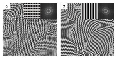
More precisely, the definition of “slightly” affine or “fully” neutral configurations generates different nano-mesh arrays for which the registration of the BCP domains of the upper layer is dictated by the conjunction of both chemical and topographical fields.
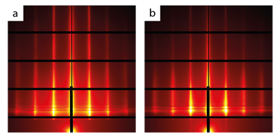
The grazing incidence small angle X-ray scattering (GISAXS) experiments performed on the SIRIUS beamline at SOLEIL were used to characterize the various nano-mesh arrays in order to retrieve the experimental configurations of the two superimposed layers and their characteristic sizes with respect to the “slightly” affine or “fully” neutral configurations (Figure 2). In particular, the GISAXS data confirms, in both cases, the formation of highly ordered nano-meshs arrays consisting of line & space patterns of 30 nm period.
This work expands the breadth of control for the self-assembly of stacked BCP layers by interplaying chemical and topographical directing methods. Accordingly, further advances in the precise manufacturing of complex structures at the nanoscale are expected by using this iterative stacking method with potential applications in lithography, optics or separation processes.