Oxide electronics -
Static and dynamic
electronic properties
of a ferroelectric device
Ferroelectric devices could be an alternative
to magnetic based memories for future
high-density data storage. Such devices
have considerable advantages: they are
non-volatile, have fast read-write times,
low energy consumption and use realistic
voltages. However, before considering future
applications based on such materials,
a better understanding of the electronic
properties of nanometer-thick ferroelectric
films is necessary. As this characterization
is often impossible with standard
techniques, we have studied ultra-thin films
of ferroelectric materials on the TEMPO
beamline, using classic and time-resolved
photoelectron spectroscopy, an ideal tool
for this kind of analysis.
In a ferroelectric device the local electric
polarization is used to store information,
either directly (FeRAMS) or by controlling
another binary material state (resistive
memories) [1].
The defining property of a ferroelectric (FE)
material is a spontaneous macroscopic
polarization which can be reversed under
an applied electric field. Switching the
polarization of such films requires a
metallic contact, raising fundamental
issues on the behavior of the interface
between the FE layer and the electrode.
The polarization leads to fixed charge
of opposite sign at the two metal-FE
interfaces. Free charge carriers in the metal
electrodes act to screen the polarization
charge, however, the screening is usually
imperfect and the residual depolarizing
field inside the FE alters the electrostatic
potential and can even suppress FE
polarization below the so-called critical
thickness [2].
The key to better understand these
systems is to probe their chemical and
electronic properties under realistic
operating conditions,
i.e.
application of d.c.
or a.c. bias in the case of a ferroelectric.
We developed a new experimental setup
to allow such
in-operando
photoemission
spectroscopy both in static and dynamic
operations at TEMPO beamline.
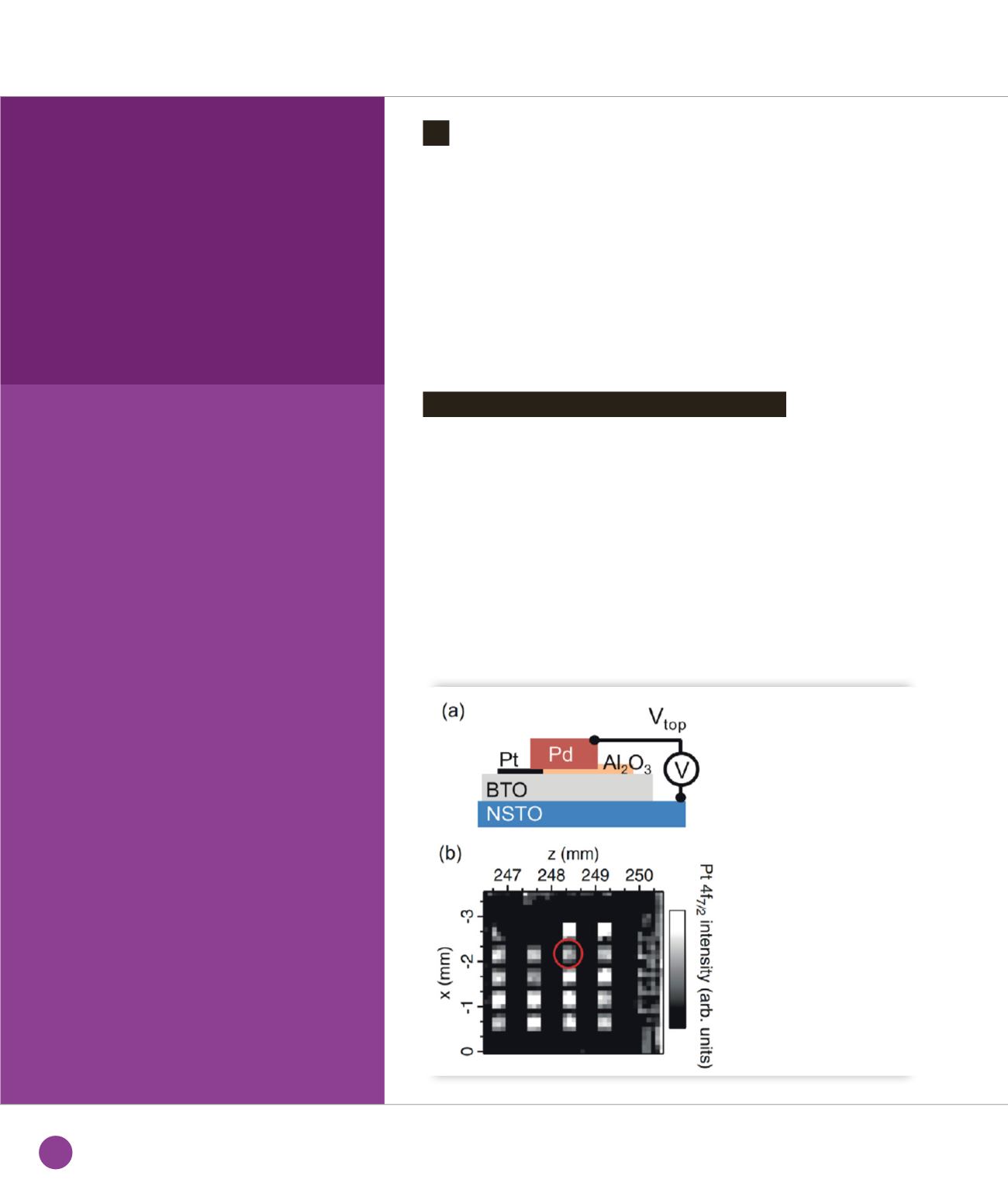
The starting point is a Pt/BaTiO
3
/SrTiO
3
:Nb
heterostructure (Pt/BTO/NSTO) grown by
Molecular Beam Epitaxy. Electrodes 300
× 300 μm² in area and 3 nm thick were
patterned by ion beam etching. Thicker
palladium pads overlapping part of the
Pt electrodes were deposited to enable
wire-bonding of the top electrodes for
biasing. A highly insulating layer of Al
2
O
3
was deposited onto bare BTO to suppress
interference of the Pd pads with the
capacitance (Figure
➊
a
). At the TEMPO
beamline, the 100 × 100 µm² beam could
be directed onto a single top electrode
located by a map of the whole sample
using the Pt absorption edge (Figure
➊
b
).
In-operando
PhotoEmission Spectroscopy
SURFACES, INTERFACES AND NANOSYSTEMS
➊
(a)
Schematic of the capacitor;
(b)
Pt 4f intensity map for the Pt/
BTO/NSTO sample showing
20 identical Pt/BTO/NSTO capacitors
(300x300 µm²) on the 5x5 mm²
surface, allowing location
of the wired capacitor (red circle).
26
SOLEIL
HIGHLIGHTS
2013


