Figure
➋
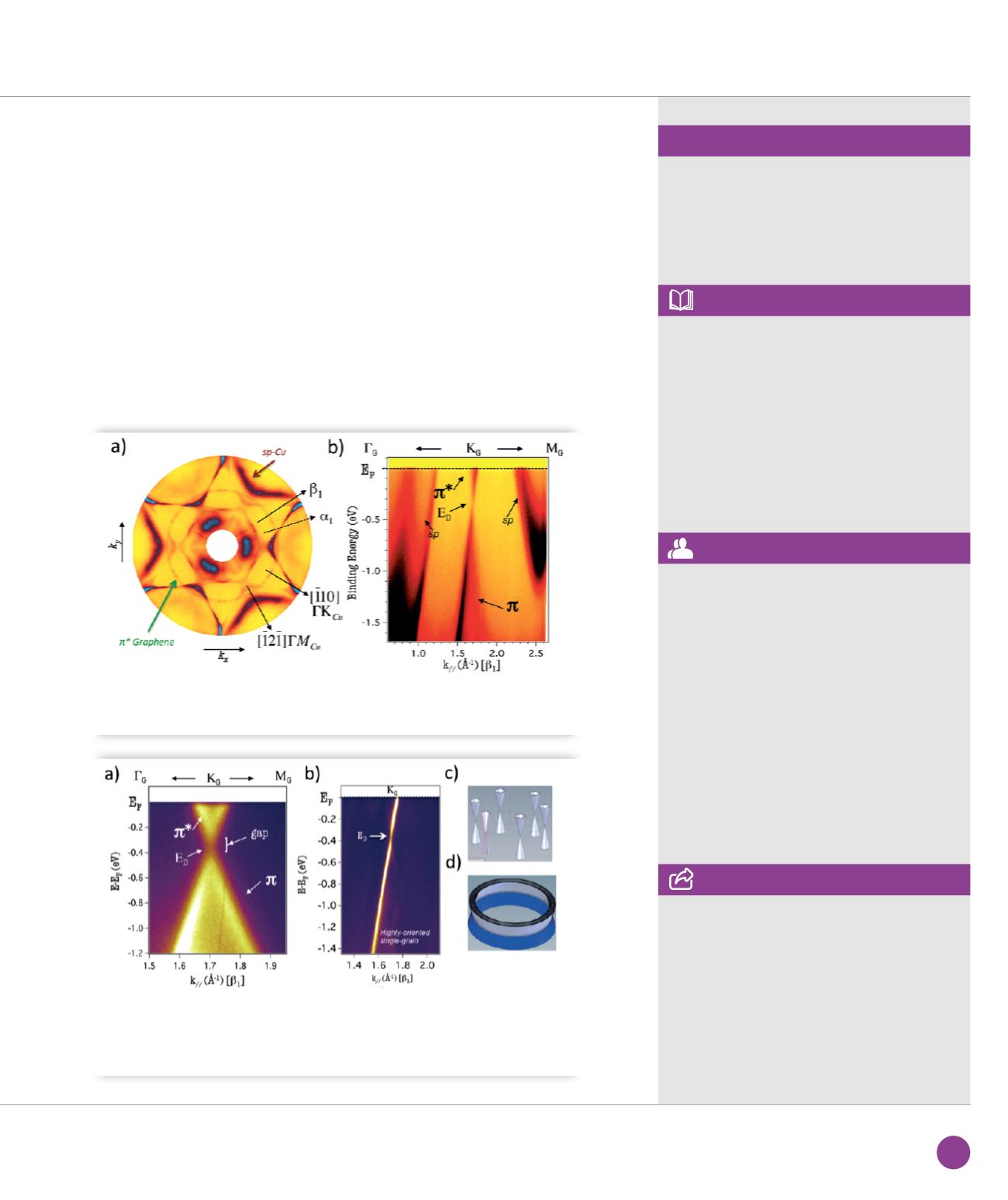
shows a Fermi surface
map subsequently measured probing
hundreds of graphene islands together.
It displays a circle instead of six bright
spots (associated to a single graphene
orientation), corresponding to the cross-
sections of graphene’s Dirac cones near
the K points of many grains randomly
oriented,. Moreover, fainter star-like
curves originated by the underlying copper
substrate electronic states.
ARPES results show, that both multi-
and single-grain ARPES spectra present
a well-defined conical Dirac dispersion,
with n-type extrinsic doping (Figure
➌
a-c
).
More importantly, the nano-ARPES gap-
size determination reveals the origin
of the discordances between experimental
gap-size values previously reported
by classical ARPES and theoretical
predictions, confirming that the graphene-
copper interaction is rather weak, which
gives rise to the opening of a mini-gap
of only
~
50 meV.
Our recent findings [4,5] certainly open
the door to a direct evaluation of the
mesoscopic structure and influence
on the electronic properties of graphene
films. These results offer new avenues
for implementing graphene in real-world
devices and exploring new phases
of electronic materials.
➋
Panel (a) shows the Fermi surface (FS) map of a graphene multi-grain film recorded at the A-box of figure 1(a).
Panel (b) displays the energy- momentum dispersion relations of
π
and
π
* bands near E
F
of graphene along the
ß
direction, using linearly polarized light of 100 eV.
ANTARES beamline
ASSOCIATED PUBLICATION
Exploring electronic structure of one-atom
thick polycrystalline graphene films:
A nano angle resolved photoemission study
J. Avila, I. Razado, S. Lorcy, R. Fleurier, E.
Pichonat, D. Vignaud, X. Wallart and M.C.
Asensio*
Scientific Reports 3 (2013): art.n° 2439
REFERENCES
[1] X. Li et al. Science 324 (2009), 1312
[2] S. Bae et al. Nat. Nanotechnol.
5 (2010), 574 J
[3] P. Y. Huang et al. Nature 469 (2011), 389
[4] J. Avila et al. Sci. Rep. 3 (2013), 2438, DOI:
10.1038/srep02439
[5] L. I. Johansson et al. Sci. Rep. 4 (2014), 4157,
DOI: 10.1038/srep041
*Synchrotron SOLEIL, l’Orme des Merisiers,
St Aubin BP48, 91192 Gif sur Yvette Cedex,
France
CORRESPONDING AUTHOR
➌
Panel (a) displays the energy-momentum dispersion relations of π and π* bands near E
F
of multi-
grain graphene film along the ß direction, using circularly polarized light of 30 eV. Panel (
b
) shows E-k
dispersion measured by nano- ARPES in a single pristine graphene grain oriented along the ß direction
(see Fig.
➋
a
). Panel (
c
) and (
d
) show the reciprocal space of single- and multi- graphene grain.
Moreover, the superposition of Dirac cones of graphene grains ramdomly oriented has been schematized.
17
SOLEIL
HIGHLIGHTS
2013


