The virtuous Graphene
goes out of the Labs,
increasing its production
up to industrial scale
Composed of a few sheets of carbon atoms,
graphene is the strongest material ever
measured, it has a thermal conductivity
more than doubled that of the diamond and
has its charge mobility, which is among the
highest of all semiconductors. But just as
their properties are remarkable, this material
likewise has accelerated the speed
to which it has left the research laboratory
for the market. The exceptional electrical
properties of graphene have been discovered
only five years ago, but today the yield
of total production of different types of
graphene is greater than 15 tons per year,
and this is expected to increase to more
than 200 tons per year within a year or two.
In SOLEIL, the ANTARES research groups
in collaboration with Wallard’s group from
the IEMN, Lille has created single large
polycrystalline graphene sheets by a simple
synthesis method and comprehensively
characterized using Nano Angle Resolved
Photoelectron Spectroscopy (NanoARPES).
Recently isolated, this material with
amazing properties began to be
manufactured following more industrial
processes. Still expensive to produce,
the graphene could soon be used for flat
screens, batteries, transistors as well as
several other applications. The idea, in the
medium term, is to replace the transparent
conductive layers of ITO (indium tin oxide),
by a layer of graphene, less fragile, which
may lend itself well to the production of
flexible displays.
Chemical vapor deposition (CVD) of single
layer graphene (SLG) on Cu has recently
emerged as a powerful technique for
realizing large scale graphene films
in a cheap readily achievable fashion,
enabling to produce continuous SLG
sheets up to meter scale fully compatible
with industrial processes [1,2]. However,
these films do not exhibit crystalline
alignment over distances critical to the
large-scale production of spatially uniform
vertical heterostructures. Specifically,
current CVD grown graphene films
are usually comprised of randomly
rotated small grains [3]
.
Indeed, for
electronic applications, when graphene
is deposited on a metal support, it is
needed to transfer it to a non-conductive
substrate after the synthesis. The whole
manipulation is difficult to control
and electronic characterization using
NanoARPES is required to detect the
eventual degradation of this polycrystalline
material as well as the optimization and
effectiveness of every step.
NanoARPES is the ideal technique
to probe the electronic structure of both
polycrystalline graphene films and Cu
substrate directly underneath it. Our
results [4] show the robustness of the
Dirac relativistic-like electronic spectrum
as a function of the size, shape and
orientation of the single-crystal pristine
grains in the graphene films investigated.
Moreover, by mapping grain by grain the
electronic dynamics of this unique Dirac
system, we show that the single-grain
gap-size is 80 % smaller than the multi-
grain gap recently reported by classical
ARPES.
In addition, it allows the investigation of
the spatial uniformity of the lattice and
electronic structures of graphene and their
correlation with that of Cu.
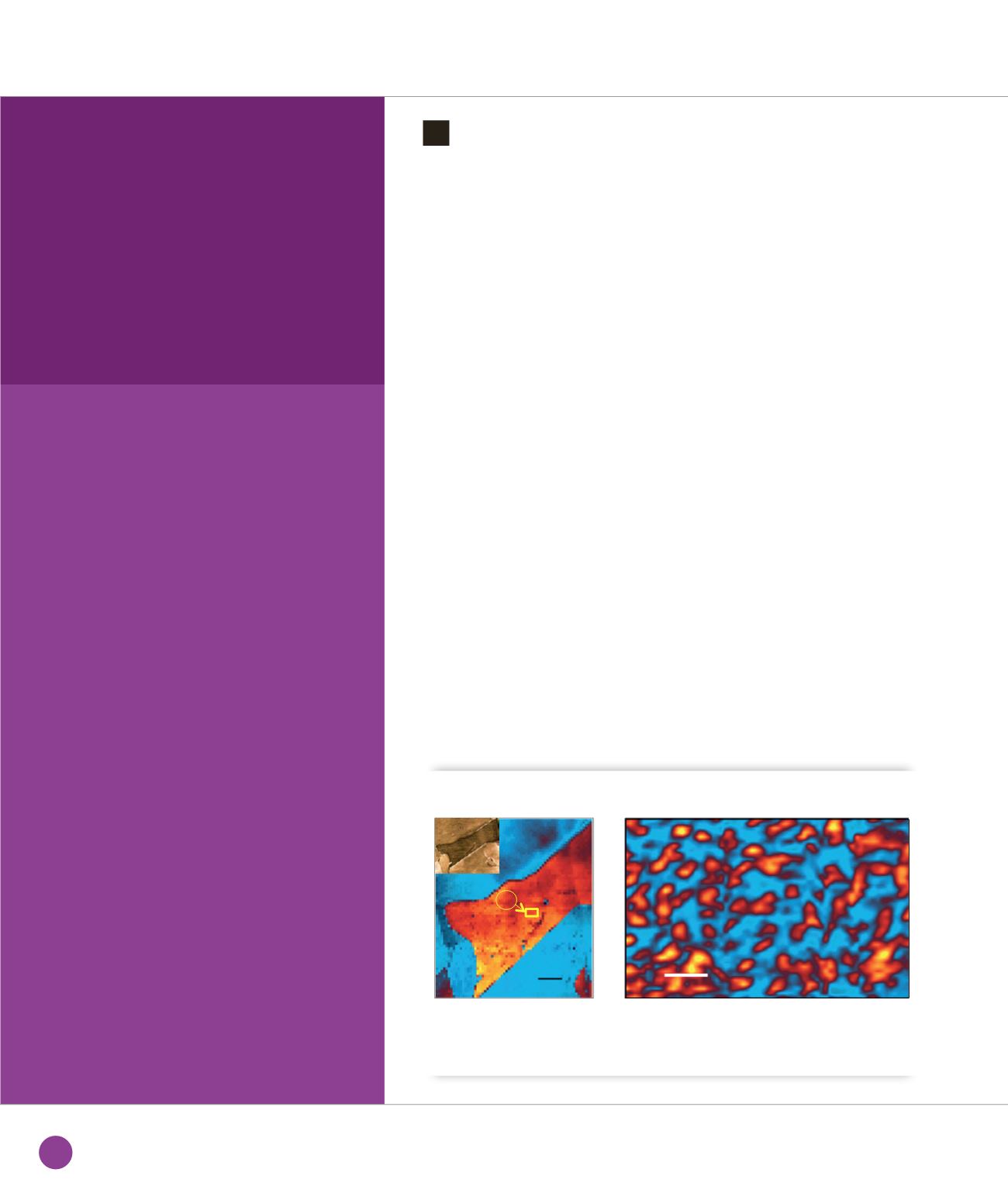
In Figure
➊
, laterally resolved nano-ARPES
data taken with a 100 nm beam spot [4]
vividly illustrate the single-crystal islands
of our graphene films as well as the
register with the granular Cu substrate.
To locate and compare different graphene
islands, we generate spatial maps (figure
1a and 1b), where an ARPES spectrum
was measured at each point in a 150 x
200 µm
2
grid.
➊
Real-space image of the copper states intensity obtained by nano-ARPES mapping presented on a linear scale
as a false-color image. The inset of panel (
a
) shows the optical image of the sample. Panel (
b
) shows real-space
images of graphene grains by monitoring the graphene states intensity at the ‘‘A’’ yellow rectangle indicated in
panel (
a
).
SURFACES, INTERFACES AND NANOSYSTEMS
500 µm
10#µm#
A#
a)#
b)#
16
SOLEIL
HIGHLIGHTS
2013


