Hydrogen/deuterium-induced puckering
of the subsurface Si atoms marks the
critical step in this nanotunnel opening.
Depending on hydrogen/deuterium
coverage, the nanotunnels are either
metallic or semiconducting as identified
by density of states (DOS) calculations and
photoemission experiments performed on
the TEMPO beamline at the 3
rd
generation
SOLEIL synchrotron. The experimental
system is optimized to monitor live the
electronic properties during hydrogen
exposure, thereby leading to identify a
semiconducting/metal/semiconducting
transition as a function of hydrogen
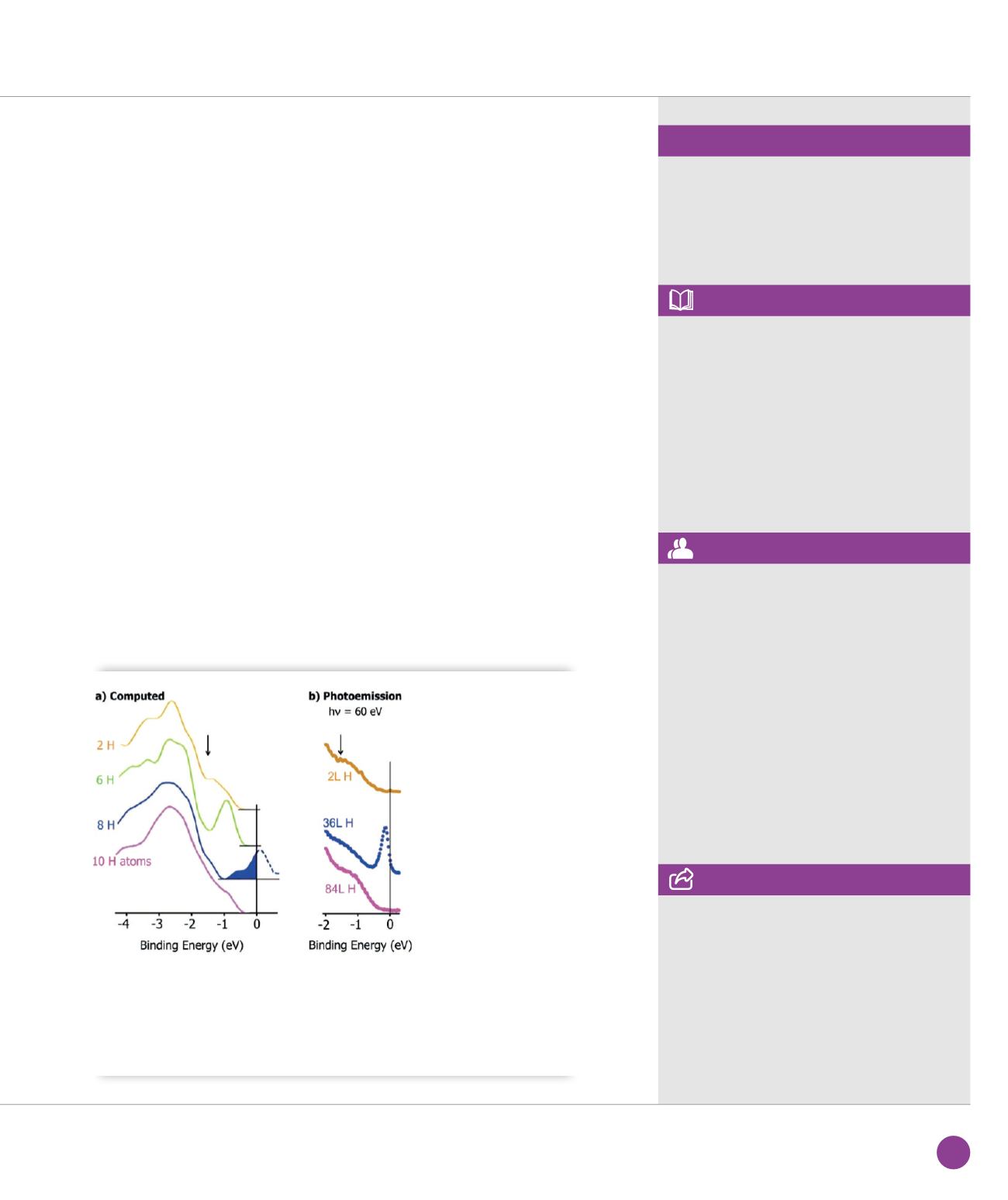
exposures as shown in Figure
➋
comparing calculated and measured
DOS, which appear to be in excellent
agreement. For the metallic nanotunnel,
the DOS build-up at the Fermi Level E
F
(shown in blue) indicating metallization
originates predominantly from the 3rd Si
atomic layer below the surface while the
combined contributions of the 1st and 2nd
Si atomic layers remain marginal.
The vibrational frequencies for the clean
and hydrogen-covered 3C-SiC(001)-3x2
surface measured by high-resolution
electron energy loss spectroscopy
(HREELS) are also in excellent agreement
with the computed ones, providing deep
insights and understanding into the
nanotunnel opening. Dangling bonds
generated inside the nanotunnel offer
a promising template to capture atoms
or molecules. These features open
nano-tailoring capabilities towards
advanced applications in electronics,
chemistry, storage, sensors or
biotechnology. Understanding
and controlling such a mechanism open
routes towards selective surface/interface
functionalization.
➋
Synchrotron radiation photoemission spectra and computed DOS for H-covered 3C-SiC(001)-3x2 surfaces.
(
a
) Computed DOS for the 2 H, 6 H, 8 H atom and 10 H atom structures integrated over the top three Si layers
and the first C layer and (
b
) SR-PES spectra recorded at photon energy of h
ν
= 60 eV in the Fermi level region
for exposures of 2L (Langmuir) H (semiconducting), 36L H (metallic) and 84L H (semiconducting) surfaces.
Note the metallic–semiconducting transition upon higher H exposures to be in very good agreement with
the calculated densities of states.
TEMPO beamline
ASSOCIATED PUBLICATION
Hydrogen-induced nanotunnel opening
within semiconductor subsurface
P. Soukiassian*, E. Wimmer, E. Celasco,
C. Giallombardo, S. Bonanni, L. Vattuone,
L. Savio, A. Tejeda, M. Silly, M. D’angelo,
F. Sirotti, and M. Rocca
Nature Communications 4 (2013) 2800 &
/
ncomms3800/pdf/ncomms3800.pdf
REFERENCE
[1] V. Derycke et al. Nature Materials
2 (2003), 253
* Commissariat à l’Energie Atomique
et aux Energies Alternatives, SIMA,
DSM-IRAMIS-SPEC, Saclay, Bât. 462,
91191 Gif sur Yvette, France
CORRESPONDING AUTHOR
29
SOLEIL
HIGHLIGHTS
2013


