Hydrogen-induced
nanotunnel opening
at the subsurface
of an advanced
semiconductor,
Silicon Carbide
Nanostructuring a surface is a key and
mandatory engineering step towards
advances in nanotechnology. A team of
scientists from the Commissariat à l’Energie
Atomique et aux Energies Alternatives,
CEA-Saclay and the Synchrotron SOLEIL,
Saint Aubin in France, from the University
of Genoa and the Consiglio Nazionale delle
Ricerche – CNR in Italy, and from the franco-
american company Materials Design Inc.,
Angel Fire, New Mexico, USA & Materials
Design sarl, Montrouge, France has shown
that hydrogen/deuterium (H/D) induces the
opening of nanotunnels below the surface of
an advanced semiconductor, silicon carbide
(SiC). This discovery is particularly interesting
in view of the remarkable properties of SiC.
These investigations have been performed
using advanced experimental tools such
as synchrotron radiation and vibrational
spectroscopy techniques, and state-of-
the-art theoretical simulations. Depending
on the H/D SiC surface exposures, these
nanotunnels undergo a sequence of
semiconducting/metallic/semiconducting
transitions. Therefore, they open very
promising prospects towards applications
in electronic, chemistry, storage, sensors
and biotechnology.
Silicon carbide (SiC), a wide band-
gap semiconductor, offers fascinating
structural, thermal, mechanical, electronic
and chemical properties, and is also
especially resistant to radiation damages.
SiC has a vast range of advanced
applications including high-power,
high-frequency, and high-temperature
electronics devices and sensors. It has
a remarkable biocompatibility making
it useful for biomedical applications.
SiC is also an especially suitable substrate
for the growth of epitaxial graphene,
with subsequent very promising potential
applications in electronics and spintronics.
Strain/stress interplay is the dominant
driving force in SiC surface ordering,
leading to more than 10 different surface
reconstructions ranging from Si-rich
to C-rich cubic SiC surfaces, and to the
self-formation of highly stable massively
parallel passive or active atomic lines
and nanowires at the surface.
Most interestingly, while H
is very well known to passivate the
surface of semiconductors, the interaction
of H/D atoms with the Si-rich 3C-SiC(001)-
3x2 surface reconstruction leads to
surface metallization, which is the first
example of H/D-induced metallization of a
semiconductor surface [1].
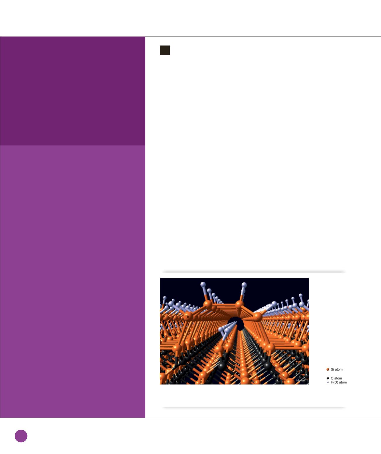
Although there are some examples
of voids or nano-cavities generated at
or below a surface, most are in the µm
or sub-µm scales, and none exhibit spatial
ordering. Here we report the first evidence
of nanotunnel opening taking place within
the subsurface region of a semiconductor,
SiC, as depicted in Figure
➊
. Such an
effect is induced by selective hydrogen/
deuterium interaction at the surface, which
possesses intrinsic compressive stress.
This finding is established combining
ab-initio
total energy and vibrational
computations using the VASP program
within the MedeA
®
computational
environment, and vibrational spectroscopy
& synchrotron-radiation-based
photoemission experiments.
➊
3D view of a Nanotunnel.
The nanotunnel opening induced by the interaction of H-atoms with the 3C-SiC(100)-
3x2 surface is represented for the 8 H metallic structure. For clarity, the empty dangling bonds are not shown.
SURFACES, INTERFACES AND NANOSYSTEMS
28
SOLEIL
HIGHLIGHTS
2013


