Universal fabrication of two-dimensional electron gases in functional oxides for future applications
Two-dimensional electron gases (2DEGs) in transition-metal oxides show remarkable properties that make them promising candidates for future applications in electronics. However, their fabrication and use are hampered by the need of growing crystalline overlayers of complex oxides thicker than 2 nm using sophisticated, expensive techniques. Now, researchers from CSNSM (CNRS/Univ. Paris-Sud), in collaboration with IEF (CNRS/Univ. Paris-Sud), LPS (CNRS/Univ. Paris-Sud), CRISMAT (CNRS/ENSICAEN), and the CASSIOPEE beamline, have shown that thermal deposition of an amorphous monolayer of an elementary reducing agent suffices to create a 2DEG in numerous oxides. This new, simpler and cheaper, fabrication route is scalable to industrial production, and ideally suited applications that rely on charge or spin injection and for the realization of mesoscopic devices.
The fabrication of two-dimensional electron gases (2DEGs) at surfaces or interfaces of transition-metal oxides lies at the heart of the emerging field of oxide electronics. Indeed, such confined metallic states can show intriguing properties, complementary to those found in semiconductor 2DEGs, such as metal-to-insulator transitions, low-temperature superconductivity, and, even more appealing for applications, magnetism and spin-polarized states.
A pressing, current goal is to make those 2DEGs suitable for applications by defining cheap and efficient processes enabling the mass production of large-area systems. However, up to now, the creation of 2DEGs in oxide heterostructures followed a single approach, requiring the growth of 20 Å or more of binary (e.g. Al2O3) or ternary (e.g. LaAlO3) oxides on SrTiO3 using highly evolved deposition techniques, such as pulsed laser deposition. Thus, not only the reproducibility of the properties of these 2DEGs depends crucially on the growth parameters, but also their fabrication is very complex, expensive and unrealistic at industrial scales. Additionally, the existence of a critical thickness of 20 Å of upper crystalline oxide layer for the onset of conductivity severely limits the control of the 2DEG’s properties, hampering applications that rely on tunneling or charge/spin injection. Similarly, 2DEGs at the surface of SrTiO3 or other oxides, discovered previously by the CSNSM team working at CASSIOPEE, are created by oxygen vacancies upon exposure to intense UV/X rays, and thus can exist only in ultra-high vacuum (UHV), to preserve the vacancies from re-oxidation, and are not suited for applications at ambient conditions.
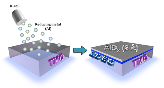
In the present work, the researchers developed a new, wholly general and extremely simple method to generate 2DEGs at surfaces of transition-metal oxides, namely, by deposition of an atomically thin film (2 Å) of pure aluminum at room temperature in UHV. Due to an efficient redox reaction, the Al pumps oxygen from the underlying oxide, transforms into insulating Al2O3 (alumina), and forms a pristine, homogeneous 2DEG in the first atomic layers of the material, as schematized in Figure 1. This overcomes the complexity of growing an oxide thin film, as the Al does not need to be oxidized before or during deposition, the requirement of a “critical thickness” of capping layer, and the necessity of strong synchrotron radiation. Moreover, as the resulting alumina film is insulating, the interfacial 2DEG is protected and can be readily used for other types of measurements and for electronic devices. The method is successfully applied to several oxides, including, as a novel application, the generation of a 2DEG in the room temperature ferroelectric BaTiO3 –Figure 2. Such hitherto unobserved coexistence of ferroelectricity and 2D conductivity in the same material is promising for functional devices using ferroelectric resistive switching.
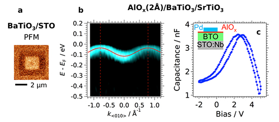
(a) Domains of opposite electric polarization, seen as concentric squares of different colors, can be written at the surface of BaTiO3 (BTO) using a conducting-tip atomic-force microscope (or piezo-force microscope, PFM).
(b) The evaporation of an atomic layer of aluminum results in the formation of a 2DEG at the BTO surface, whose electronic band dispersion was measured using ARPES at CASSIOPEE.
(c) Capacitance–voltage curve on the same AlOx(2 Å)/BaTiO3 interface, showing the butterfly shape characteristic of a ferroelectric hysteresis. A Pd circular pad and the Nb:STO substrate were used as top and bottom electrodes, respectively.
These results represent a breakthrough towards the realization of 2DEGs in functional oxides using a universal, inexpensive procedure that is both suitable for the fabrication of electronic devices, even at the nanoscopic and mesoscopic levels, and accessible to industrial production.