First Evidence of Silicene Nanoribbons Synthesized on an Insulator
Silicene, a single plane of silicon atoms organized in a honeycomb pattern, is, along with graphene - the equivalent of silicene, but with carbon - one of the new 2D materials that have attracted great interest due to its high potential to be integrated in modern nanotechnologies. However, the production of free-standing* silicene has proven to be a huge challenge.
In this study, a first experimental demonstration of the formation of a silicene monolayer on an insulating NaCl thin film is reported, pointing to the formation of silicene nanoribbons decoupled from the metal substrate by the thin NaCl layer. This work opens real perspectives for the integration of silicene as a 2D material in electronic devices.
A few years after the discovery of graphene, an exceptional electronic conductor, a lot of attention has been paid to the research on new two-dimensional (2D) materials. Indeed, the integration of graphene in electronic devices has certain limitations due to the inherent lack of “band gap” in its electronic structure, resulting in the absence of semiconducting properties in graphene. This limitation could be overcome by using materials that can form 2D structures, be semiconducting and have an electronic structure similar to that of graphene. This is the case of silicene or germanene (Germanium atoms).
The first experimental evidence of the existence of a 2D silicon atomic layer with honeycomb structure (silicene) was obtained on Ag(111) surface in 2010. Soon after, the growth of silicene on many other metal substrates was reported in the literature. However, the question of the electronic structure of silicene remains open due to the existence of a strong coupling between silicene and the metal substrate which results in the destruction of its intrinsic properties.
For the first time, teams from ISMO (France), Synchrotron SOLEIL (France), CEA-SPEC (France), Mohamed 5 University (Morocco) and the University of Central Florida (USA), have succeeded in growing silicene nanoribbons on an insulating NaCl film by molecular beam epitaxy. Atomic resolution scanning tunneling microscopy (STM) images, recorded at low temperature (78 K) in ISMO, show silicon nanoribbons organized in a honeycomb pattern (Figure 1a). A computational study performed using Density Functional Theory (DFT) is in agreement with the experimental findings (Figure 1b).
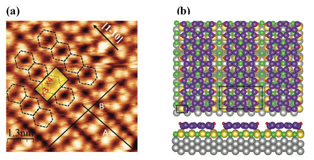
(a) STM image showing honeycomb-shaped silicon nanoribbons.
(b) Top view (up) and side view (down) of the structure obtained by theoretical simulation of the silicene nanoribbons on NaCl/Ag(110), after full relaxation. Ag, Cl, Na, H and Si atoms are colored, respectively, in gray, green, yellow, red and blue purple. The (1x1) and the (3x4) cells are indicated by the small and large rectangles, respectively.
High-resolution X-ray photoelectron spectroscopy (XPS) experiments were performed at TEMPO beamline using the synchrotron radiation. Cl 2p and Na 2s core level spectra were recorded after Si deposition on NaCl/Ag(110). As shown in Figure 2, fitting the Cl and Na spectra requires only one spin–orbit split component. This means that Na and Cl ions have only one chemical environment (Na surrounded by Cl atoms and Cl atoms surrounded by Na). This is evidence of a weak interaction between the NaCl film and Si as well as between the NaCl film and the silver substrate. Similarly, the Si 2p spectrum has only one spin–orbit split component, indicating that the silicon atoms are all equivalent in having only one chemical environment. Thus, the Si atoms are adsorbed on top of the NaCl film and the Si-NaCl interaction is weak.
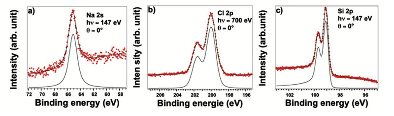
a) Na 2s,
b) Cl 2p, recorded after deposition of 1 monolayer of NaCl on Ag(110);
c) Si 2p, recorded after deposition of 1 monolayer of silicon on top of the NaCl/Ag(110). All the spectra are recorded at normal emission (0°). Dots correspond to the raw data and the overlapping black line corresponds to the best fit. For each spectrum, the component giving the best fit is indicated in black.
Extended X-ray absorption fine structure (EXAFS) measurements recorded at the Si K-edge carried out at LUCIA beamline have provided complementary information on the local structure of the 2D silicon layer grown on NaCl/Ag(110) surface. They give a precise determination of the interatomic distance between the excited atom (here Si) and its neighbors. These measurements, obtained both on bulk silicon and on silicon layer grown on NaCl/Ag(110) surface, confirmed that that the Si atoms are located on top of the NaCl film, not directly on the Ag surface.
Considering all the information from the STM, XPS, and EXAFS studies, we conclude that silicon atoms adsorb on the ultrathin NaCl film to form a 2D layer with a local silicene-like structure that is sufficiently decoupled from the silver substrate.
The existence of such a decoupling, guaranteeing the preservation of silicene properties, makes it possible to envisage the integration of silicene in devices that could exploit both its semiconductor qualities and the high mobility of its electrons, for faster and miniaturized electronics.
* free-standing: 2D materials are synthesized on the surface of a material called "substrate". The interactions between the substrate and the atoms of the 2D material can modify the properties of the latter, which is why researchers try to reduce these interactions. When they are reduced to a minimum, one speaks of a free-standing 2D material.