The effects of confinement (of electrons) on the surface states of a topological insulator
Today, the total data storage capacity in the world is between 10 and 50 zettabytes (1021), and this value could double every two years. Research into new materials that would enable higher data storage density and lower power consumption is very active. Scientists at the CASSIOPEE beamline are studying promising materials: topological insulators with the chemical formula Bi1-xSbx
In 2017, digital technology accounted for less than 3% of the world's electricity consumption, but this share is expected to double by 2025; some studies predict that it could even rise to 30% by 2030. Spintronics, electronics that also use the 'spin' of the electron in addition to its charge, offers the prospect of less energy-intensive components. One of its greatest successes has already been to gain three orders of magnitude in the density of data stored on a hard disk thanks to the high sensitivity of giant magnetoresistance sensors. Now the focus is on developing non-volatile, low-power magnetic memories.
These magnetic memories store information in the form of a magnetisation of a magnetic layer: a magnetisation in one direction is a 1, while the magnetisation in the opposite direction is a 0. To invert a magnetic bit the properties of the electron are used: one "simply" needs to inject a current with the appropriate "spin polarisation" into the magnetic layer. The spin of the electron is, along with its charge and mass, its third intrinsic property; sensitive to magnetic fields, the spin can be roughly seen as a kind of tiny magnet carried by the electron, and it exists in two "orientations", up and down. A spin-polarised current is made up of electrons whose spins are massively oriented either up or down. The problem is to be able to create these spin-polarised currents.
The importance of topological insulators
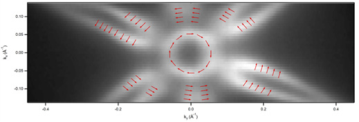
This is where topological insulators come in. These are electrically insulating materials, but their surface (on some atomic planes) is conductive. The most peripheral electrons are free to circulate on the surface of the material, they are electrons that are very far from the atomic nuclei and therefore not very attached to the atoms; their binding energy is low or even zero. Confined to the first atomic planes of the material, they form a "two-dimensional metal". Their momentum (the vector indicating their direction of motion in classical mechanics) is therefore also parallel to the surface and can be described by two components (kx and ky). Angle-resolved electron photoemission spectroscopy allows to measure an 'intensity map' of these surface states as a function of the kx and ky components, for electrons with zero binding energy (Fermi surface). As these kx and ky components are quantized, this map tells us which states are allowed for these most peripheral electrons of atoms. It is shown in Figure 1 for one of the Bi1-x Sbx compounds studied on the CASSIOPEE beamline.
Why such a measurement?
Firstly, to check whether the intensity map of the surface states reflects the symmetries of the crystal. The Bi1-x Sbx compounds have a hexagonal lattice surface: indeed, a six-petalled flower-shaped Fermi surface with a hexagonal core is observed. Secondly, and more importantly, because the theory predicts that this Fermi surface must have a spin texture, i.e. a regular arrangement represented on figure 1 by the red arrows which symbolise the direction of the spins for the observed electronic states. The spins wind in one direction on the hexagonal core and in the opposite direction on the petals. This texture should allow a very efficient charge current-spin current conversion: the passage of a 'classical' (charge) current in one direction should generate a spin-polarised current in the perpendicular direction.
In order to be incorporated into an electronic device, these materials need to be grown as thin films on substrates compatible with these applications. In this study, Bi1-x Sbx samples are fabricated by evaporating Bismuth (Bi) and Antimony (Sb) onto a Silicon substrate. The x-composition of the alloy can be varied (to change the shape of the Fermi surface) by varying the relative evaporation rates, as well as the total film thickness. One of the surprising results is the variation of the electronic structure with the thickness of the film. The study shows that this confinement of electrons in a thin film influences the properties of the material, and that it should be taken into account to optimise its performance when used in spintronics.
Is this material really efficient for spin current/charge current conversion? This question was the subject of another study on CASSIOPEE, the results of which are also to be published. To be continued!