Versatile variable temperature insert at the DEIMOS beamline for in situ electrical transport measurements
The V2TI project (Versatile Variable Temperature Insert) was designed to enhance the sample environment capabilities of theDEIMOS beamline by adding multiple electrical wiring to the sample. It is now possible to electrically polarize the sample, measure electrical voltages or currents across the sample while performing x-ray measurements under DEIMOS standard conditions; from 20K to 300K and under up to 2 Tesla magnetic field. It also allows to operate a device (e.g. a piezo-electric motor) or any applications that require electrical wiring under these same conditions.
This new asset will greatly benefit researches both in material and in physical science. This development was spurred by the multifunctional properties of novel materials such as multiferroics, which exhibit simultaneously several ferroic orders, and hold great potential for new devices application. The most promising ones include ferroelectric and magnetic ordering, for which XAS/XMCD can bring valuable information.
The V2TI project
The V2TI project involved two research groups, the IPCMS institute (Institut de Physique et Chimie des Matériaux de Strasbourg) and the DEIMOS beamline at SOLEIL. The challenge was to achieve 12 wire connections on a sample holder both electrically insulated (to allow for total electron yield detection mode) and thermally conductive (to perform low temperature experiments), while allowing for sample transfer under UHV condition.
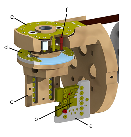
The electrical insulation of the sample holder with a good thermal contact at low temperature is achieved by a sapphire ring separating the head of the V2TI from the rest of the cold finger. The electrical contacts at the level of the sample holder (Figure 1) are obtained by multilayer printed circuit boards (PCBs, Figure 1-d and 1-e) connected by small spring dots (Figure 1-f).
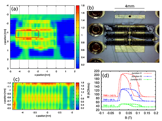
The sample itself is fixed onto a chip (Figure 1-a and 1-b) which is then clipped ex situ onto the sample holder prior to UHV transfer. The sample chip is provided ahead of the beam time to the users who can then electrically bind their devices to the sample chip in their laboratory (Figure 2-b). After checking the electrical connections the device is ready for operation and measurements.
Testing the versatile variable temperature insert
The different capabilities of the insert have been tested:
- A temperature probe used as a sample has permitted the determination of the temperature at the sample position, Tsample= 20 K.
- The electrical insulation (better than 200 GΩ) is compatible with the measurement of TEY signal as small as 100 fA.
- The capabilities of the insert for the measurement of multifunctional sample have been tested on MgO-based Magnetic Tunnel Junctions (MTJs), that currently represent an essential cornerstone of spintronics, with inroads into spin-torque nano-oscillators, MRAM and magnetic sensors. The MTJs are fabricated at IPCMS according to clean room techniques and using the following stack grown at the Institut Jean Lamour (IJL), Nancy: glass / Ta (5 nm) / Co (10 nm) / IrMn (7.5 nm) / FeCoB (4 nm) / MgO (2.5 nm) / FeCoB (5 nm) / Ta (5 nm) / Pt (3 nm).
After an alignment (Figure. 2a and 2c), we present in Figure. 2d a set of R(H) curves [resistance (R) of the sample as a function of the magnetic field (H)] measured at T = 300 K and with a sample bias of V = 5 mV that shows TMR values for several devices ranging from 49% to 140%, as expected.
Prospective
For multiferroic system (in our case, system combining ferro-electricity and ferromagnetism) the idea is to use the properties of XAS/XMCD for electronic and magnetic characterization while polarizing the sample. Performing XAS/XMCD measurements while we change the electronic and magnetic properties of the sample will improve our understanding of the electronic and magnetic interplay.
For the MTJs, the idea is to measure device properties by performing resistivity measurements, while the atoms of the junction absorb x-rays with synchrotron-grade brilliance. That reveals unparalleled insight into the electronic properties of only those atoms that drive the MTJ’s operation and spintronic performance which should propel our understanding of how devices operate.