In situ study of the synthesis of TiS2 films by alternating deposition of organic & inorganic molecules
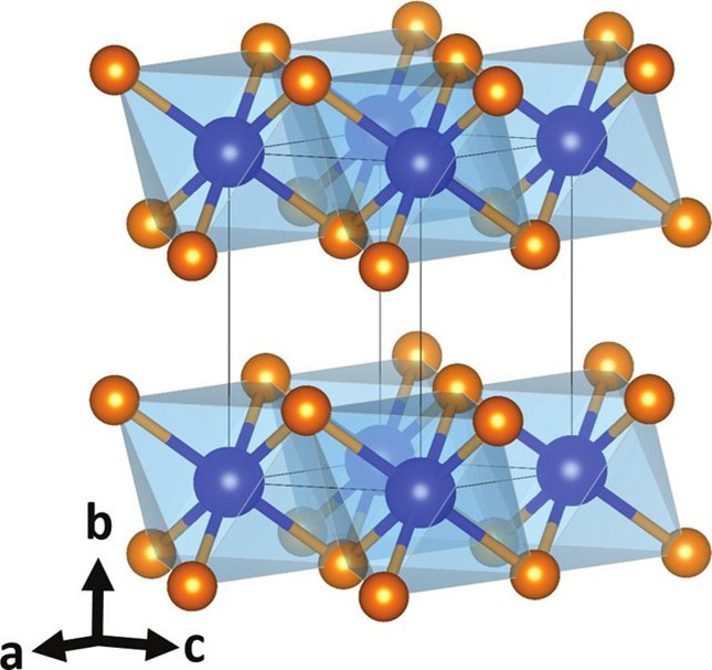
Lamellar Metal Dichalcogenides* have emerged as a class of exceptional materials which exhibits remarkable electronic and chemical properties on the scale of a few monolayers.
Scientists from Grenoble and Lyon report the two-step synthesis of lamellar titanium disulfide (TiS2) thin film on thermal silicon oxide wafer.
A set of analysis techniques implemented on the SIRIUS beamline of SOLEIL, associated with ellipsometry, allowed to observe and control in situ the whole synthesis process.
Titanium disulfide (TiS2) is the lightest and less expensive member of the Transition Metal Dichalcogenides (TMDs) family. Its electrical properties lead to many potential applications such as positive electrodes in Li-ion batteries or supercapacitors, among other fields of applications (optics, thermoelectrics, photovoltaics, …).
However, the lack of scalable fabrication methods of continuous, crystalline and textured (characteristic relative to the lateral dimension and the orientation of the layers in the film) ultra-thin films, on possibly non-crystalline substrates with a large surface, is a sizeable bottleneck for their full deployment.
Scientists from LMGP, CEA-Leti, CEA-IRIG (Grenoble Alpes University), CP2M, IRCELyon, IPVF and the SIRIUS beamline succeeded to synthesize continuous and textured graphite-containing TiS2 ultra-thin films on silica-terminated wafer by using an innovative two-step approach. Furthermore, the implementation of in situ observation and analysis techniques on the SIRIUS beamline allowed them to study the growth and annealing mechanisms, and to accelerate the development of the manufacturing process.
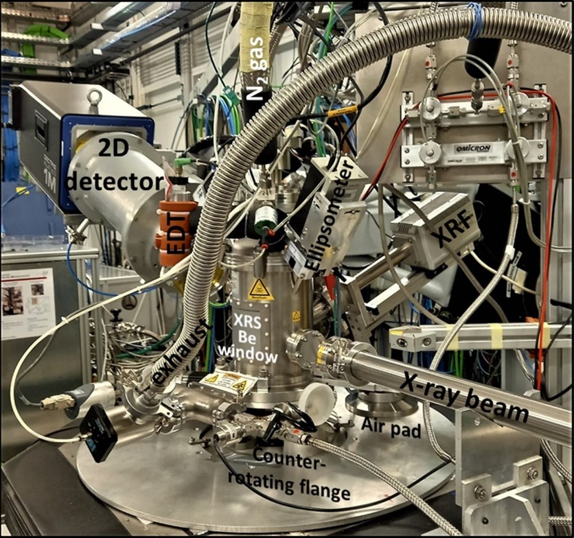
The two-step process was developed in a custom-built portable reactor which mounts onto the 6-axis tower of the NewportTM diffractometer installed at the beamline SIRIUS (Figure 2).
The set-up allows to use a complementary suite of in situ analysis techniques, i.e. x-ray reflectivity, x-ray fluorescence and absorption spectroscopies, as well as in-plane x-ray scattering.
By the end of the first step, an amorphous film (Ti thiolate type) is obtained at 50°C by reaction between an inorganic metal precursor (tetrakis(dimethylamido)titanium) and an organic molecule containing sulfur (1, 2-ethanedithiol, a less toxic source of sulfur than H2S gas) alternately deposited on a 100 nm thick SiO2/Si planar substrate (ALD/MLD process for "atomic layer deposition /molecular layer deposition").
The unique features of the SIRIUS beamline allow the simultaneous recording of the X-ray fluorescence emission intensities of titanium and sulfur, allowing their respective contents to be monitored during the manufacturing process (figure 3). Similarly, the X-ray absorption spectra of Ti and S could be recorded from the early stages of film deposition, thus providing information on the evolution of the local atomic environment of the two atoms.
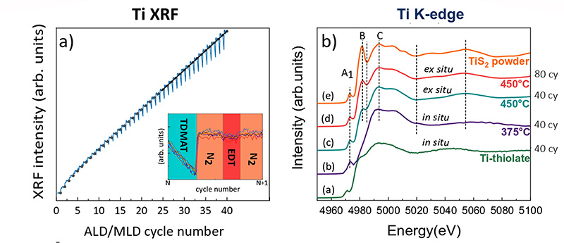
(a) Ti x-ray fluorescence emission intensity
(b) Ti x-ray absorption spectra
Upon thermal annealing the thin film transforms into TiS2 layers parallel to the SiO2 substrate surface (texture). The quality of the films was assessed by a combination of analytical techniques including X-ray absorption spectroscopy (Figure 3 (b)), Raman spectroscopy (Figure 4 (a)), transmission electron microscopy (Figure 4 (b)) and photoemission spectroscopy performed post-fabrication at CEA-Leti.
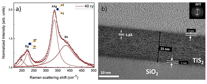
(a) Raman scattering spectra
(b) cross-sectional transmission electron microscopy image of 40-cycle ALD/MLD annealed thin films
The latter showed the presence of TiS2, together with adventitious carbon. The film texture was confirmed at a macroscopic scale by X-ray absorption linear dichroism.
Moreover, resistivity measurements and spectroscopic ellipsometry suggest that the TiS2 thin films grown on SiO/Si substrates behave as heavily-doped semiconductors.
Conclusion
In the quest for large-scale deposition methods for the fabrication of textured lamellar metal chalcogenides on amorphous substrate, the scientists have adopted a synthesis strategy based on the alternating deposition of a metal precursor molecule with an organic precursor molecule followed by a specific annealing and applied it to the preparation of titanium disulfide (TiS2). The fine control of the whole synthesis process could be achieved by in situ synchrotron studies during the 2-step process, thorough ex situ structural and chemical characterizations, and chemical experimental modeling on high surface area silica beads.
This work was achieved in the frame of the ANR project ANR-18-CE09-0031.
*Transition-metal dichalcogenide (TMD or TMDC) monolayers are materials that exist in the form of layers consisting of only 3 planes of atoms, separated by a van der Waals gap which limits the interaction between the layers; we refer to 2D materials. Their physical properties are very anisotropic. They are of the type MX₂: M is a transition metal atom, X a chalcogen atom, the plane of atoms M is sandwiched between the two planes of atoms X.