Imaging shape and strain in nanoscale engineered semiconductors for photonics by coherent x-ray diffraction
Today, quantum dots, nanowire arrays, and buried solid-state nanostructures are examples of components used in innovative functional devices for photonics and optoelectronics, including photonic crystals, with applications like optical computers, or more efficient photovoltaic cells.
For the first time, through coherent X-ray diffraction imaging in Bragg geometry (Bragg CDI), an international team of researchers from SOLEIL (CRISTAL & SIRIUS beamlines), the Institute for Photonics and Nanotechnologies (CNR, Rome, Italy), The Sapienza Università di Roma (Italy), the University of Nottingham (UK), SLAC National Accelerator Laboratory (USA), and the Laboratoire de Physique des Solides (Orsay) has imaged the size, shape and inner strain field within micro- and nanostructures of GaAsN embedded in a hydrogenated-GaAsN/GaAs epilayer.
The results, published in Nature Communications Materials, demonstrate that Bragg CDI can be used for direct evaluation of the structural quality of single embedded or buried photonic micro- and nanostructures, even for the cases where conventional microscopies cannot be carried out.
Traditionally, photonic devices can be fabricated by lithographic processes (“top-down” methods), producing highly uniform structures with poor optical properties; or by self-assembly processes in highly strained heterostructures (“bottom-up” methods), which produce high efficiency devices although losing control in their spatial distribution. Both approaches are therefore limiting the performance of photonic devices. A third route was recently demonstrated by the researchers, consisting in exploiting the effects of hydrogen irradiation in dilute nitrides (particularly GaAsN). H-irradiation produces N-H stable complexes that change the crystal lattice parameters and the band gap energy. Therefore, by incorporating H in selected areas of the crystal, a modulation of the optical properties can be introduced in a fully controlled manner. The researchers team used this approach to create different non hydrogenated structures of GasAsN embedded in a hydrogenated-GaAsN/GaAs epilayer (see figure 1a), both with different band gap energy.
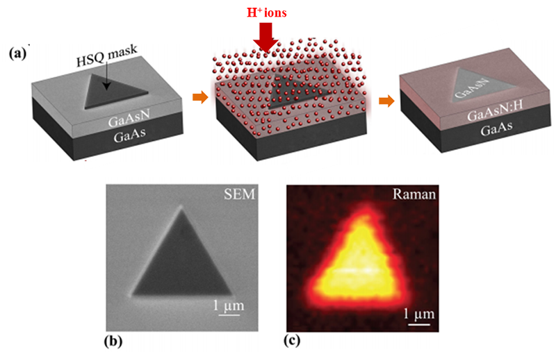
Yet, there is a lack of non-destructive high resolution characterization methods that give direct access to the size, shape, and strain field of these nanostructures, which are vital parameters to fully control the properties and response of these photonic devices. In order to characterize such embedded structures, traditional microscopy methods are limited. Micro-Raman and microphotoluminescence (PL) do no offer enough spatial resolution to image the sharpness of these structures (see figure 1c); and they do not give access to the strain distribution within the microstructures, which alters dramatically their optical properties. On the other hand, electron microscopies are not suitable because of the very low contrast between the hydrogenated and native parts of the device. Furthermore, the structures need to be buried below the surface to obtain high optical quality: thin samples have to be prepared then, introducing additional strain and other artifacts.
These issues can be efficiently tackled with Bragg coherent X-ray diffraction imaging (Bragg CDI), a novel technique developed in the early 2000s that requires an intense coherent X-ray source, typically from a 3rd (or 4rth) generation synchrotron undulator, such as the SOLEIL CRISTAL and SIRIUS beamlines. Bragg CDI allows obtaining the 3D structure (size, morphology, composition, but also displacement and strain fields and defects) of micro- and nanostructures (from 100 nm upwards) with a spatial resolution of approximately 5-100 nanometers and sensitivity to fluctuations in the displacement field in the picometer range. Therefore, Bragg CDI is a very sensitive technique for imaging strain within micro- and nanostructures.
.
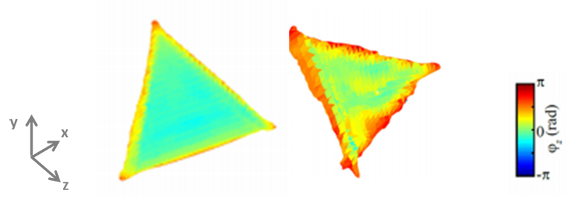
The researchers used the Coherent Diffraction setup at CRISTAL beamline, an instrument devoted to performing Bragg CDI measurements at the highest resolution, and the SIRIUS beamline in an innovative layout. The team obtained 3D high resolution images of the embedded GaAsN 5-micron and 500-nm size photonic structures, with a resolution of 51 and 22 nm respectively (see figure 2), which is twelve times better than the resolution obtained by optical imaging. In addition, thanks to Bragg CDI the strain field was also obtained for all the structures. From the results, the distribution of the atom displacement can be considered quite constant in the bulk of the structures, and increases dramatically only close to the borders. These findings were fully corroborated by Finite Element Analysis simulations. This result enables the direct evaluation of the structural quality of the single micro- and nanostructures produced via the selective hydrogenation method, and paves the way towards the extension of these fabrication methods for nanophotonic devices.
The team results enable the direct evaluation of the structural quality of the single micro- and nanostructures produced via the selective hydrogenation method; and pave the way towards the extension of these fabrication methods for nanophotonic devices. Furthermore, this work opens the door to the application of Bragg CDI as a characterization method of choice for buried and embedded photonic devices; and particularly in the next future, with the SOLEIL synchrotron upgrade, that will allow studying much smaller structures in a similar way.