Free layers of graphene obtained after the insertion of silicon on silicon carbide
Graphene is the most studied material to prepare electronics in the future. Among the methods used to produce some, one lies on the intercalation of silicon upon a substrate of silicon carbide.
French scientists managed to create and characterize quasi free standing nano-layers graphene from a substrate of silicon carbide they doped with silicon. The electronic properties of intermediate nano-junctions obtained during the process revealed potential applications as Schottky diodes.
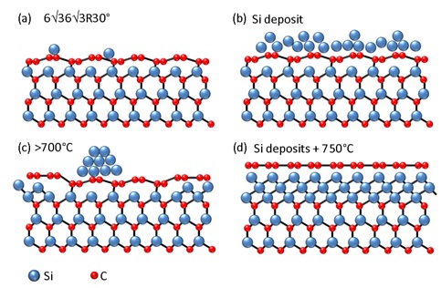
Silicon carbide is a semiconductor initially studied for its specific electronic properties: high thermal conductivity, wide band gap, high field breakdown strength and high carrier saturation velocity. It has recently become the object of a renewed interest, especially in its 6H-SiC form as a substrate to produce graphene, the material thought to revolutionize electronics in the future. Despite its high structural quality, graphene electronic properties are suffering a charge transfer between graphene layer and subsurface, leading to a drop in intrinsic doping and charge-carrier mobility. To overcome this problem, different approaches to form quasi free standing graphene layers have been studied based on intercalation with atoms of Hydrogen, Oxygen, Fluorine, Gold, Lithium, Germanium and Silicon. The last one is actually compatible with present electronic technology and offers the possibility to be easily oxidized and passivate the decoupled graphene layers represents one of the most promising approaches.
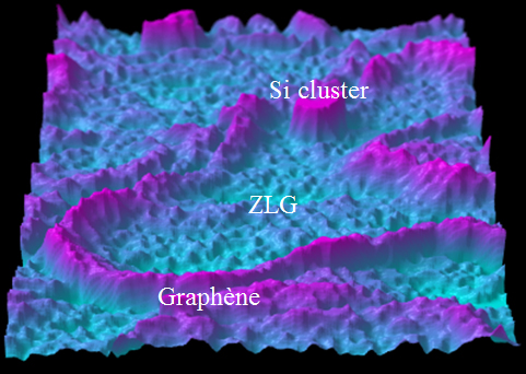
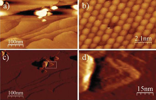
A French team from SOLEIL synchrotron, Institut des Nanosciences de Paris (CNRS/UPMC), Service de Physique de l’Etat Condensé (CNRS/CEA) and Laboratoire de Chimie Physique-Matière et Rayonnement (CNRS/UPMC) studied the intercalation mechanism of Si in 6H-SiC, in order to produce single layers graphene. Their works recently published in the Carbon review show that silicon presents two way of diffusion on surface during the intercalation process. Either it migrates through the surface defects and contributes to a progressive decoupling of the ZLG from the substrate, either it agglomerates at the surface to form silicon clusters. After sequences of silicon deposition followed by annealing at 750°C, agglomerated silicon disappears. It is indeed located at the interface of SiC and a monolayer of graphene, which is almost free-standing.
This phenomenon has been observed by the combination of high resolution photoemission spectroscopy (HRPES), angle resolved photoemission spectroscopy (ARPES) performed on the TEMPO beamline as well as with atomic force microscopy and low energy electronic diffraction. During the process, scientists have also been observing an intermediate state: metal semi-conducting junctions with potential applications as Schottky diodes.