Following the electron pathway within a 2D material
Optoelectronic devices, such as LEDs, lasers, and cameras, play a central role in our daily lives. These devices rely on controlling light and its interaction with matter, typically modulated by a simple mechanism: an electric bias. Therefore, understanding how this bias affects a given material is essential for optimizing its performance. Although the first transistors based on 2D materials, such as transition metal dichalcogenides, appeared in 2011, a relevant gauge to probe locally the electric fields has been largely lacking until now. In collaboration with the ANTARES beamline, a team from INSP (Paris) has mapped the electric field in these materials during operation at the nanoscale, paving the way for their rational optimization.
The study of 2D materials, such as transition metal dichalcogenides (TMDCs), has become central to the development of advanced optoelectronic devices. When reduced to monolayers, these materials exhibit remarkable electronic properties, including high carrier mobility and tunable energy gaps*, making them ideal candidates for next-generation nanoelectronics. However, their integration into devices significantly alters their electronic structure due to interactions with the surrounding dielectric environment and the influence of external electric fields. This presents challenges in understanding and optimizing their behavior at the nanoscale. The influence of external electric fields, as seen in field-effect transistors (FETs), is particularly critical. Yet, the precise local impact of these fields on the device energy landscape remains poorly understood due to the limitations of existing local probing techniques.
This work introduces an advanced method using scanning photoemission microscopy (SPEM) in operando conditions to map the energy landscape of 2D TMDC-based FETs, providing new insights into how electric fields and material properties interact during device operation. This technique, available at the ANTARES beamline of the SOLEIL synchrotron, exploits the high spatial resolution of the focused X-ray beam (< 1 µm) and the capability to bring electrical contacts directly to the sample, enabling in operando measurements.
In collaboration with a group from IPCMS, the INSP team fabricated three-electrode transistors with a WSe2 flake as the channel. The transistor design allows for independent control of charge carrier speed and density through the application of two separate voltages. This device geometry, combined with the advanced SPEM technique, enabled the researchers to investigate how these applied voltages modify the electronic structure of the semiconductor.
The approach has enabled precise sub-μm resolution mapping of the bias-modified energy landscape and the vectorial mapping of electric fields—both out-of-plane (induced by the gate bias) and in-plane (due to the drain-source bias) (see Figure 1b). The technique proves to be a sensitive local probe, providing critical insights into the device design, as well as the geometry, thickness, and morphology of the 2D material flakes. These factors all influence the electric field distribution and the current flow within the device channel.
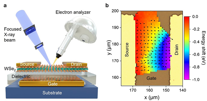
Moreover, SPEM allows for the determination of the conversion factor between the applied gate bias and the material's potential and reveals how the vertical gate field is primarily screened at the interface with the basal plane of the 2D material (with a screening length of a few nm). In TMDCs, strong screening of the gate effect occurs with increasing thickness. This screening limits the gate's ability to control charge density in thicker flakes, thereby affecting overall device performance. This phenomenon highlights the importance of material thickness and geometry when designing optimized devices based on 2D materials.
This work provides a direct measurement of the potential profile within a device, a process previously inferred only through electrical measurements. It paves the way for a more rational optimization of devices and for directly quantifying the impact of non-idealities. Building on these findings, future research will expand the application of in operando SPEM to a broader range of 2D materials beyond TMDCs, including complex van der Waals heterostructures. These materials hold potential for even more customizable and efficient electronic devices, with a focus on how geometry configurations and interlayer interactions affect electric field distribution and device performance. This effort will continue under the ANR project E-map, led by the teams at INSP and the ANTARES beamline.
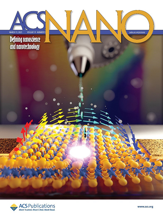
The article describing these results is featured on the cover of the March 2025 issue of ACS Nano (Figure 2).
*bande interdite : correspond à l’énergie qu’un électron du matériau doit acquérir pour devenir libre de circuler – dans le cas d’un semi-conducteur, c’est l’énergie à lui fournir pour qu’il passe de l’état isolant à l’état conducteur. Cette énergie peut être fournie, entre autre, par la lumière.