DIFFABS
DIFFABS : Combining X-Ray diffraction and absorption to study a large variety of materials
The range of instrumental techniques that can be used on this line concerns numerous sectors of fundamental research and finalized applied research (oil industry, nuclear field , metallurgy) among which the science of materials and chemistry hold a predominant position. In particular, in situ studies of the transformations in materials at ultra-high temperature will be the domain of excellence of this line. The interest of coupled absorption, or coupled - diffraction measurements on powders or monocristalssingle crystals, is to ensure that both experiments are carried out on the same zone of the sample, in absolutely identical physico-chemical conditions (temperature, pressure, reactive atmosphere around the sample), which is very important for establishing correlations between the information provided by both types of measurements in the case of complex materials or materials under extreme conditions.
Beamline news
All DIFFABS's news
SOLEIL Highlights 2025
SOLEIL Highlights 2024
Team
Videos
All DIFFABS's videos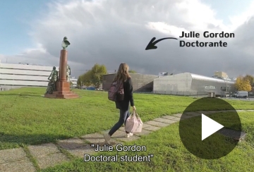
Julie's PhD thesis – episode 2 - Musée des Arts et Métiers - Storage facility
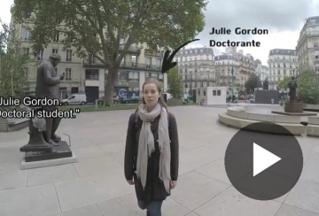
Julie's PhD thesis – episode 1 - Musée des Arts et Métiers
Technical data
- Energy range
-
3-23 keV for standard beam mode
3-19 keV for microbeam mode
- Energy Resolution (∆E/E)
-
∆E/E ~ 10-4
- Source
-
Bending magnet
- Flux at the first optical element
-
1.1014 ph/s/0.1%bw @ 8 keV / 500mA ring current
4. 1013 ph/s/0.1%bw @ 20 keV / 500mA ring current
- Optics
-
Mains optics
Two bendable mirrors for harmonics rejection and meridian (vertical) focusing
- Si(111) Double crystal monochromator (DCM) with bendable 2nd crystal for sagital (horizontal) focusingFocusing optics for microbeam mode
- Kirkpatrick-Baez (KB) mirror (~ 10μm)
- Circular Fresnel Zone Plate (sub-10μm beam size)
- Sample Environment
-
- 6+2 circles diffractometer (kappa geometry + analyzer crystal). Heavy load and cumbersome sample environment can be accommodated.
- motorized (x,y,z)-stage allowing the precise positioning and mapping of the sample +-12mm (or+-5cm, +-10cm, +-15cm)
- Several heating systems :
(laser heating + levitating chamber (study of melting of glasses, oxides and ceramics up to T ~3000 °C)
conventional furnaces for powders, thin films and bulk (up to
1300°C)- compact Peltier stage (T = -20°C to +50 °C)
- biaxial tensile machine for stretchable thin films
- optical microscope (sample visualisation and pre-alignment) for μbeam experiments
- Beam characteristics on sample (flux and size)
-
standard mode
- several 1012 ph/s @ 8kev / 500 mA ring current
~250x300μm2 FWHM, 0.24 x 3.5 mrad2, vert. × horiz. with Si(111) DCM
microbeam mode
- 109-1010 ph/s @ 8kev / 500 mA ring current
~10x10μm2 FWHM, 2 x 1 mrad2, vert. × horiz. using KB
- Detectors
-
2D detectors : CIRPAD and XPAD S140
- Zero- dimensional (YAP or LaCl3 scintillators)
- Zero- dimensional (Avalanche Photo Diode, APD)
- thin Si diodes (I0 monitors),
- diodes (transmitted beam) for X-ray absorption experiments
- 4-element SDD: silicon drift detector for X-ray fluorescence+ additionnal (XPAD, MAR345 image plate, 4element SDD …) on-loan basis from Detectors Group, shared with other beamlines.
Scientific Opportunities
| Materials Science |
|
|---|---|
| (Semiconductor) nanostructures |
|
| Soft condensed matter |
|
| Cultural Heritage |
|
| Biology, Biomaterials | Pathological calcifications |
| Environnement et science de la Terre |
| Materials Science | - in-situ studies of mechanical properties of materials (crystalline metallic layers, multilayers, polymers, …) under bi-axial tensile stress. - in-situ structural studies of glasses, oxides and ceramics at very high temperatures (by XRD and XAS combination) - phase transitions on different materials - 1beam studies (local probe) for structural properties : 1XRD, 1XAS, 1XRF and combination |
|---|---|
| Biology, Biomaterials | - Pathological calcifications |
| (Semiconductor) nanostructures | - local properties in lithographed semiconductor epitaxial thin films, quantum wells/wires/dots, nanostructures (Laterally resolved High resolution XRD by using x-ray focused beams). - III-V semiconductor multilayers for optoelectronics |
| Soft condensed matter | - in-situ studies of mechanical properties of polymers (rubbers) under uniand bi-axial stress. |
| Imaging / cartography / local probe analysis | - local probe (10 1m and sub-101m X-ray spot) imaging / mapping / analysis with various contrast mechanisms and information (diffraction, fluorescence, spectroscopy). - Large variety of samples: crystalline or amorphous materials, nanomaterials, polymers, biological samples, archeological artifacts, … |
| Art and cultural heritage / archeology | - In situ monitoring of dechlorination treatment of marine archaeological artefacts by combination of microbeam techniques - Determination of the polychromy techniques of the archaic Greek ceramic decorations |
Art and cultural heritage / archeology
.