Aller au menu principal
Aller au contenu principal
Venir à SOLEIL
Annuaire & contacts
Accès intranet
FR
EN
À propos de SOLEIL
Nous connaitre
Nous rejoindre
Recherche
Recherche Interne
Collaborations et projets de recherche
Sources et Accélérateurs
Plateformes
Savoir-Faire
Supports aux utilisateurs
Laboratoire de Métrologie Optique (LMO)
Lignes de lumière
Par domaines d'énergie
Localisation des lignes
Utilisateurs
Demande de temps de faisceau
Évaluation des projets
Préparer son expérience (scientifique)
Préparer son expérience (administratif)
Après l'expérience
ORGanisation des UtilisatEurs de SOLEIL (ORGUES)
Entreprises
Caractérisation de matériaux
Développements technologiques et valorisation
Autres prestations specifiques
Nos engagements
Documentation
Publics
Partager la culture scientifique
Se documenter
Découvrir nos vidéos
Visiter SOLEIL
Entrez votre recherche
Accueil
>
Actualites
Actualites
Sciences en direct
Vie de SOLEIL
Lignes de lumière
R&D et supports
- Tout -
Alignement
Détecteurs
Divers
Electronique
Groupe Théorique
Informatique
Instrumentation
Laboratoire Biologie
Laboratoire Chimie
Laboratoire Matériaux
Laboratoire Matériaux Anciens
Laboratoire Microfluidique
Optique
Sources
Sections scientifiques
- Tout -
Heliobio
MMI
AtMol
MC
MatD
Surface
Domaines de recherche
- Tout -
Matériaux avancés
Biologie
Santé
Phase Gaz
Matière sous conditions extrêmes
Nano-objets
Matière condensée
Sources
Instrumentation
Interfaces (solides/gaz/liquides)
Techniques d'analyse
- Tout -
Photoelectron emission
Imaging
Scattering
Emission or Reflection
Absorption
Diffraction
Lithography
Ion Spectroscopy
Theory
Domaines d'application
- Tout -
Agrosciences
Matériaux anciens
Agroalimentaire
Bâtiments - Travaux publics
Chimie
Cosmétique
Énergie
Environnement et éco-industries
Matériaux
Microélectronique et nanotechnologies
Transports
Médecine
Date
Start date
Date
E.g., 20/04/2024
End date
Date
E.g., 20/04/2024
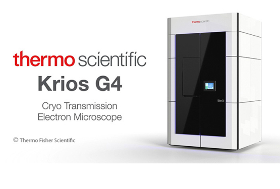
Publié le 11/04/2024
Un cryo-microscope électronique de 300 keV disponible à SOLEIL en 2025
Lundi 18 mars 2024, plus de 8 tonnes de matériel ont été livrées à SOLEIL. Il s'agit des pièces du nouveau cryo-microscope électronique qui sera mis à disposition des utilisateurs, sur base d'appel à projets, à partir de 2025.
Lire la suite
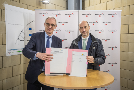
Publié le 15/04/2024
Communiqué de presse - La chaleur fatale du Synchrotron SOLEIL va chauffer 1000 logements...
L’EPA Paris-Saclay et SOLEIL ont signé une convention de partenariat, le 15 avril 2024, pour capter et valoriser la chaleur fatale* produite par le Synchrotron. Elle alimentera un réseau d’échange de...
Lire la suite
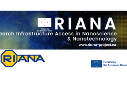
Publié le 03/04/2024
Lancement du projet européen RIANA
Un hub pour les nanosciences et les nanotechnologies
Lire la suite
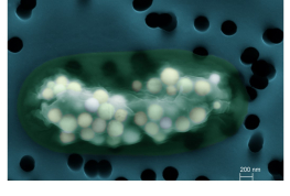
Publié le 26/03/2024
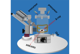
Exploration atomique de précipités calcaires à l’intérieur de bactéries
Certaines bactéries forment des granules calcaires micrométriques à l’intérieur de leurs cellules, stockant ainsi du calcium et du carbone. Leur fonction reste inconnue mais les cellules dépensent de...
Lire la suite
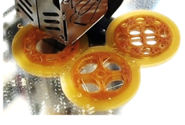
Publié le 26/03/2024
Des impressions 3D comestibles : sur ANATOMIX, tomographie X rapide en temps réel des...
L’impression 3D de pièces comestibles à base de biopolymères naturels ouvre de nouvelles perspectives dans le domaine pharmaceutique, dans le but d’obtenir des structures sur-mesure permettant la...
Lire la suite
Publié le 26/03/2024
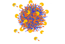
Recherche d’alternatives aux opioïdes : Des nanoparticules de promédicaments analgésiques...
La crise des opioïdes constitue aujourd'hui un défi majeur pour la santé mondiale. Les opioïdes sont les analgésiques les plus puissants et les plus largement utilisés, mais ils présentent de graves...
Lire la suite
Publié le 26/03/2024
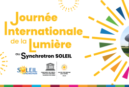
Journée Internationale de la Lumière 2024 – Visite du Synchrotron SOLEIL avec entrée...
Depuis 2018, le 16 mai a été déclaré par l’UNESCO Journée Internationale de la Lumière. Avec un peu d’avance sur cette date, SOLEIL ouvre à nouveau ses portes pour la cinquième édition de cette...
Lire la suite
Publié le 19/03/2024
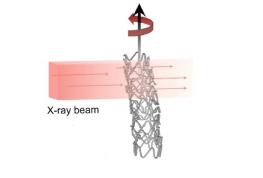
Sur la ligne ANATOMIX, étude de la résorption de stents biorésorbables in vivo
Les maladies coronariennes, principale cause de mort subite, sont aujourd'hui traitées à l'aide de stents expansibles qui ouvrent les artères pour la circulation sanguine. Mais ces stents ne peuvent...
Lire la suite
Publié le 06/03/2024
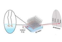
Percer les mystères d’une nouvelle approche de synthèse des films ultraminces de TiS
...
Dans le paysage en constante évolution de la science des matériaux, la quête de techniques innovantes pour fabriquer des films ultraminces de dichalcogénures de métaux de transition
1
(en...
Lire la suite
Publié le 04/03/2024
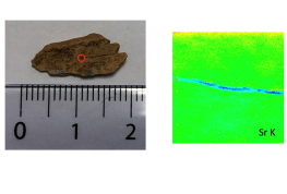
Sur les traces de l’ivoire de mammouth, un témoin de la préhistoire
Il y a 40 000 ans, les humains préhistoriques ont utilisé l’ivoire de mammouth pour façonner les premières statuettes et fabriquer les premiers instruments de musique découverts à ce jour. L’ivoire...
Lire la suite
Publié le 04/03/2024
Des réactions chimiques contrôlées et ciblées, grâce à la surface de l'eau
Dans la chimie moderne il est très compliqué de contrôler, pour une réaction donnée, l’endroit précis où va se dérouler cette réaction sur les molécules impliquées. C’est cependant crucial :...
Lire la suite
Publié le 20/02/2024
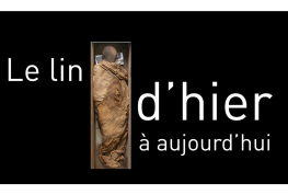
Vidéo - Le lin, d’hier à aujourd’hui
Quel est le point commun entre des bandelettes de momie et la coque d’un bateau ? Les deux contiennent des fibres de lin ! Très appréciée des Égyptiens, cette matière végétale aux nombreuses...
Lire la suite